Converters: Comparators, DACs, and ADCs
Instruments 3.2
Learning Objectives
By the end of this session, you should be able to:
Explain how comparators form the “front end” between analog sensors and digital logic.
Design simple alarm and hysteresis (Schmitt trigger) circuits with comparators.
Compute the output of unipolar and bipolar DACs and select resolution (number of bits).
Compute the digital output of an ADC for a given analog input and reference.
Compare successive‑approximation and dual‑slope ADCs and predict their conversion time.
Analyze how conversion time limits the maximum signal frequency and why sample‑and‑hold is needed.
Describe frequency‑based A/D conversion using counters and V‑to‑F converters.
These objectives map to practical instrumentation tasks: alarm design, driving actuators from a microcontroller, choosing ADC/DAC resolutions, and understanding the constraints of data acquisition hardware. Emphasize that every measurement or actuator they use in embedded systems ultimately passes through these building blocks.
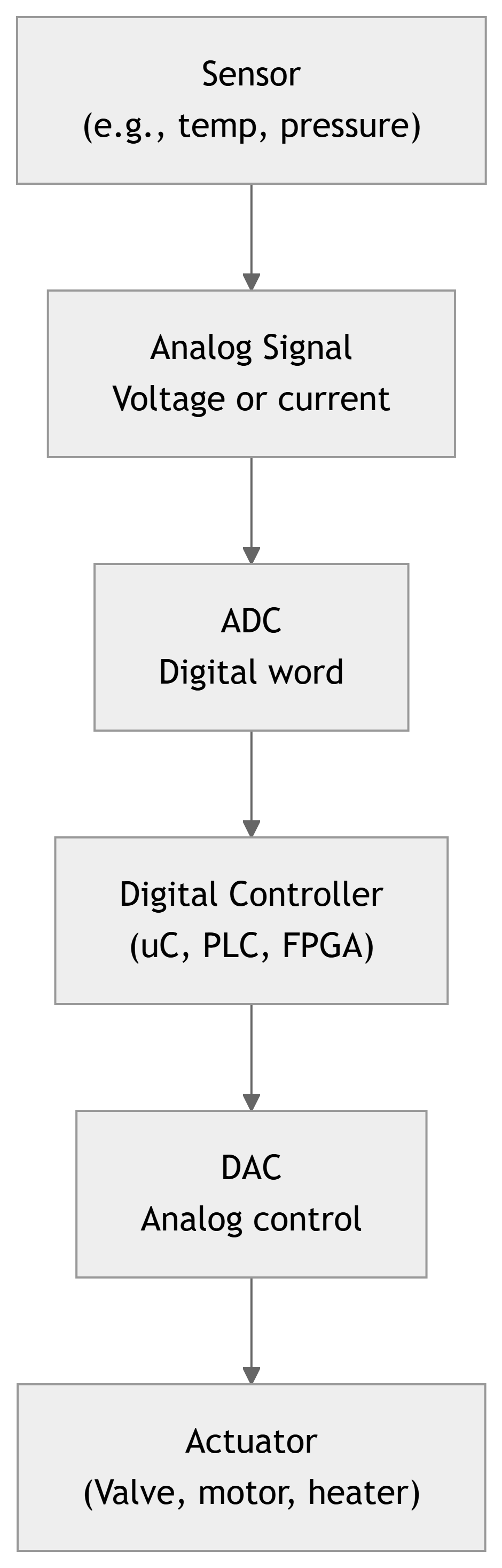
Big Picture: Why Converters Matter in ECE
Sensors mostly give analog outputs (voltages/currents).
Microcontrollers, FPGAs, PLCs work with digital words .
Actuators often need analog drives (valves, motors, heaters, etc.).
So we need:
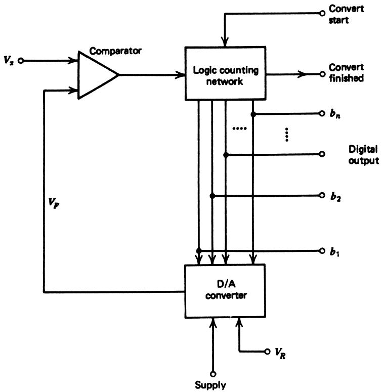
ADC : analog → digital (measurement path)DAC : digital → analog (actuation path)Comparator : simplest analog/digital boundary (1‑bit ADC)
In process control:
A temperature/pressure sensor → ADC → controller → DAC → valve / heater.
Correct converter selection and design determines accuracy, speed, and stability.
Walk through a typical control loop: temperature sensor in a chemical reactor, analog signal to ADC, digital control, DAC output to a valve. Point out that comparators are like 1‑bit ADCs used for alarms or simple threshold logic, while full ADCs/DACs handle multi‑bit precision.
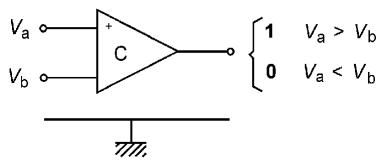
3.1 Comparators: Concept
A comparator outputs a digital 1 or 0 depending on which input voltage is larger.
Think of it as a one‑bit ADC with a fixed threshold .
Given inputs \(V_a\) and \(V_b\) :
If \(V_a > V_b\) → output = logic 1 (high).
If \(V_a < V_b\) → output = logic 0 (low).
Common uses:
Alarm and interlock circuits.
Zero‑crossing detection (e.g., AC line).
Building blocks inside ADCs and DACs.
Emphasize: unlike an op‑amp used with feedback, a comparator is intended to saturate to rails and switch quickly. It’s not for linear amplification, but for making decisions: above or below threshold.
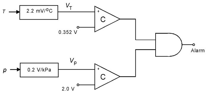
Comparator Alarm Example (Process Control)
Spec: Trigger an alarm if - Temperature \(T > 160^\circ\mathrm{C}\) - AND pressure \(P > 10\ \mathrm{kPa}\)
Transducers:
Temperature: \(V_T = 2.2\ \mathrm{mV}/^\circ\mathrm{C} \cdot T\)
Pressure: \(V_P = 0.2\ \mathrm{V}/\mathrm{kPa} \cdot P\)
Compute trip voltages:
\(V_{T,\text{trip}} = 2.2\ \mathrm{mV}/^\circ\mathrm{C} \times 160^\circ\mathrm{C} = 0.352\ \mathrm{V}\) \(V_{P,\text{trip}} = 0.2\ \mathrm{V}/\mathrm{kPa} \times 10\ \mathrm{kPa} = 2.0\ \mathrm{V}\)
Use:
One comparator for temperature > 0.352 V.
One comparator for pressure > 2.0 V.
One AND gate to combine the two alarms.
Explain that each comparator compares the sensor signal to a fixed reference (built from a resistor divider). The digital outputs feed an AND gate that drives a buzzer or microcontroller input. This is a typical process‑safety interlock.
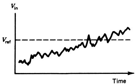
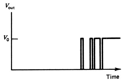
Comparator Noise Problem: “Jiggling” Output
Noisy signal near the threshold:
Result:
If the input crosses the reference slowly or has noise , the comparator may rapidly switch between high and low.
In real systems this can:
Chatter relays/valves.
Create multiple interrupts to a microcontroller.
Generate spurious alarms.
Solution: Hysteresis (Deadband) → The comparator must cross a higher threshold to turn on than to turn off.
Relate this to a thermostat that doesn’t turn the heater on/off every second as the temperature jitters around the setpoint. Hysteresis introduces a small band where no switching occurs.
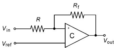
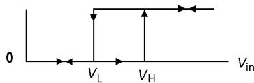
Hysteresis Comparator (Schmitt Trigger)
For \(R_f \gg R\) :
Output goes high when: \[V_{\text{in}} \ge V_{\text{ref}} = V_H\]
Once high, output will stay high until input falls below: \[V_{\text{in}} \le V_{\text{ref}} - \frac{R}{R_f} V_0 = V_L\]
Hysteresis width (deadband): \[\Delta V = V_H - V_L = \frac{R}{R_f} V_0\]
Walk through the feedback intuition: when output goes high, the feedback slightly raises or lowers the effective threshold at the input (depending on topology), producing two distinct switching levels. Highlight that by choosing \(R/R_f\) we tune how large a band of noise we can tolerate.
Hysteresis Design Example (Splashing Tank)
Spec:
Level sensor: \(V = 20\ \mathrm{mV/cm} \cdot h\)
Comparator output: high (5 V) whenever level \(h \ge 50\ \mathrm{cm}\)
Splashing causes \(\pm 3\ \mathrm{cm}\) fluctuation (noise).
Compute:
Nominal reference at 50 cm: \[V_{\text{ref}} = 20\ \mathrm{mV/cm} \times 50\ \mathrm{cm} = 1.0\ \mathrm{V}\]
Splashing amplitude: \[\Delta V_{\text{noise}} = 20\ \mathrm{mV/cm} \times 3\ \mathrm{cm} = \pm 60\ \mathrm{mV}\] Total “noise range” = 120 mV.
Choose hysteresis slightly larger, say \(150\ \mathrm{mV}\) .
Use these in the Figure 10 hysteresis comparator with \(V_{\text{ref}} = 1.0\ \mathrm{V}\) .
Stress the design flow: specify noise level → choose deadband > noise → back‑compute resistor ratio. Then pick convenient standard resistor values. This pattern reappears in many comparator designs.
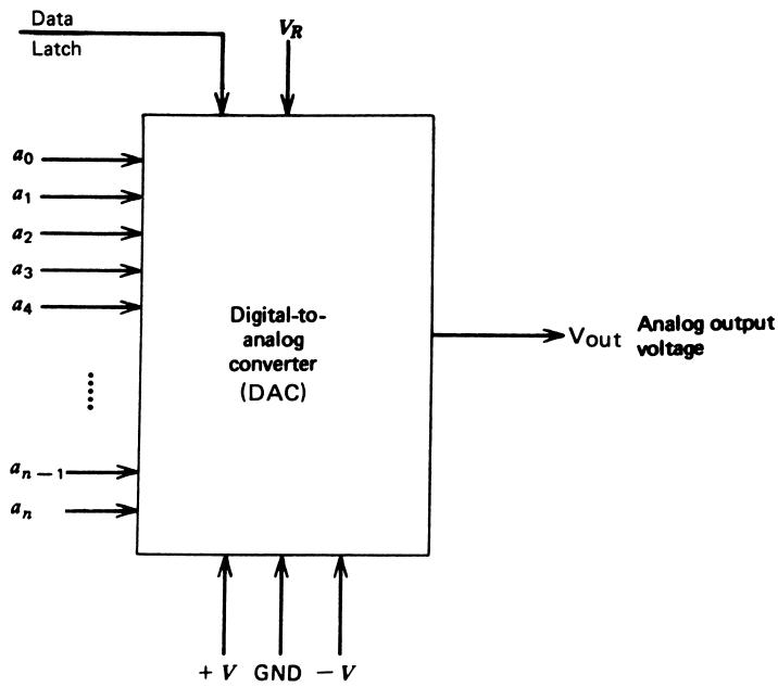
3.2 Digital‑to‑Analog Converters (DACs): Overview
A DAC converts a digital code (binary word) into an analog voltage or current .
Input: \(n\) ‑bit binary word \(b_1 b_2 \dots b_n\) (MSB to LSB).
Output: a staircase analog voltage (or current) over a defined range.
Two main types in this section:
Unipolar DAC : output range \(\approx 0\) to \(+V_R\) (or some fraction).Bipolar DAC : output range \(\approx -V_R/2\) to \(+V_R/2\) .
Uses in ECE:
Driving actuators (valves, motors, VCOs, etc.) from microcontrollers.
Setting analog reference levels under software control.
Generating waveforms, test signals (e.g., arbitrary waveform generators).
Relate to a typical microcontroller board with an external SPI DAC: students may have used it to set an analog control voltage. Here we’re deriving the math behind that black box and resolution limits.
Unipolar DAC Transfer Function
For a unipolar \(n\) ‑bit DAC with reference voltage \(V_R\) :
Binary word \(b_1 b_2 \dots b_n\) with \(b_i \in \{0,1\}\) :
\[
V_{\text{out}} = V_R \left[ b_1 2^{-1} + b_2 2^{-2} + \dots + b_n 2^{-n} \right] \tag{5}
\]
Interpretation:
The DAC treats the binary input as a fraction in [0,1) .
Each bit contributes a weighted fraction of \(V_R\) .
Maximum output when all bits are 1:
For \(n=4\) : \[V_{\max} = V_R(2^{-1}+2^{-2}+2^{-3}+2^{-4}) = 0.9375 V_R\]
For \(n=8\) : \[V_{\max} = 0.9961 V_R\]
Alternative, easier formula using decimal equivalent \(N\) :
\[
V_{\text{out}} = \frac{N}{2^n} V_R \tag{6}
\]
where \(N\) is the base‑10 value of the input code.
Make sure students see that the maximum is slightly below \(V_R\) because the binary fraction never reaches 1 exactly, only \((2^n-1)/2^n\) . Eq. (6) is often easier to use—stress conversion of hex/binary to decimal N.
Example: 8‑bit DAC Output
Given:
8‑bit DAC, \(V_R = 5.0\ \mathrm{V}\)
Input code: \(\mathbf{10100111}_2\) = A7H
Convert input to decimal:
\(N = 167_{10}\) , and \(2^8 = 256\) .
Use Equation (6):
\[
V_{\text{out}} = \frac{167}{256} \cdot 5.0 = 3.2617\ \mathrm{V}
\]
So the digital word A7H produces ≈ 3.26 V at the DAC output.
Practice: compute \(V_{\text{out}}\) for input 80H (10000000₂).
\(N = 128\) , \(V_{\text{out}} = (128/256)5 = 2.5\) V.
Encourage students to internalize the idea that the MSB roughly halves the range, so 10000000₂ gives about half of \(V_R\) .
Solve Equation (6) for \(N\) :
\[
N = 2^n \frac{V_{\text{out}}}{V_R} = 1024 \cdot \frac{6.5}{10} = 665.6
\]
\(N\) must be an integer → can’t get exactly 6.5 V.
\(N=665\) → 299H → 6.494 V\(N=666\) → 29AH → 6.504 V
Only way to get exactly 6.5 V is to adjust \(V_R\) .
Use this to demonstrate quantization : the analog range is broken into discrete steps; many desired analog values fall between steps. Here we see the requirement that some inaccuracy is unavoidable unless we change the reference or increase resolution.
Bipolar DAC: Offset‑Binary
Some DACs output from negative to positive voltage (bipolar).
A common representation is offset‑binary :
\[
V_{\text{out}} = \frac{N}{2^n} V_R - \frac{1}{2} V_R \tag{7}
\]
\(N\) ranges from \(0\) to \((2^n - 1)\) .When \(N = 0\) : \[V_{\text{out}}(\min) = -\frac{V_R}{2}\]
When \(N = 2^n - 1\) : \[V_{\text{out}}(\max) = \frac{1}{2}V_R - \frac{V_R}{2^n}\]
So the output is nearly symmetric about 0 V but slightly less than \(+V_R/2\) at the max code.
Example 10
10‑bit DAC, \(V_R = 5\ \mathrm{V}\)
04FH → \(N = 79\) → \[V_{\text{out}} = \frac{79}{1024}\cdot 5 - 2.5 \approx -2.114\ \mathrm{V}\]
2A4H → \(N = 676\) → \[V_{\text{out}} \approx \frac{676}{1024}\cdot 5 - 2.5 \approx 0.801\ \mathrm{V}\]
Zero output occurs when Equation (7) = 0 → \(N = 2^{n-1} = 512 = 200\mathrm{H}\) .
Connect offset‑binary to 2’s complement: microcontrollers often use 2’s complement, but the DAC might expect offset‑binary, so conversion may be needed in firmware. Offset‑binary is simpler in analog hardware because it’s just a DC shift.
DAC Resolution
The smallest change in output for a 1‑LSB change in input is:
\[
\Delta V_{\text{out}} = V_R 2^{-n} \tag{8}
\]
This is the voltage resolution of the DAC.
Example:
5‑bit DAC, \(V_R = 10\ \mathrm{V}\) → \[\Delta V_{\text{out}} = 10 \cdot 2^{-5} = 0.3125\ \mathrm{V}\]
Design question: How many bits to get \(\Delta V \le 0.04\ \mathrm{V}\) with \(V_R = 10\ \mathrm{V}\) ?
Solve:
\[
0.04 = 10 \cdot 2^{-n} \Rightarrow 2^{-n} = 0.004 \Rightarrow n \approx 7.966
\]
So \(n = 8\) bits is sufficient.
Check:
\[
\Delta V_{\text{out}} = 10 \cdot 2^{-8} = 0.03906\ \mathrm{V} < 0.04\ \mathrm{V}
\]
Students should be comfortable doing back‑of‑the‑envelope calculations: “I want steps of about X volts; with V_R = Y, how many bits?” This is essential for sizing data converters in real designs.
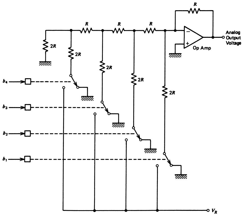
DAC Internal Structure: R–2R Ladder
Uses only two resistor values: \(R\) and \(2R\) .
Each bit controls a switch feeding either reference or ground into the ladder.
Network analysis shows output matches Equation (5) / (6).
Benefits:
Easy to fabricate in IC processes (only two precision resistor ratios).
Good matching → good linearity.
Scales easily with number of bits.
You don’t need to derive the ladder math fully in class, but emphasize the idea: each branch contributes half the weight of the previous, summed via the op‑amp to form the analog output.
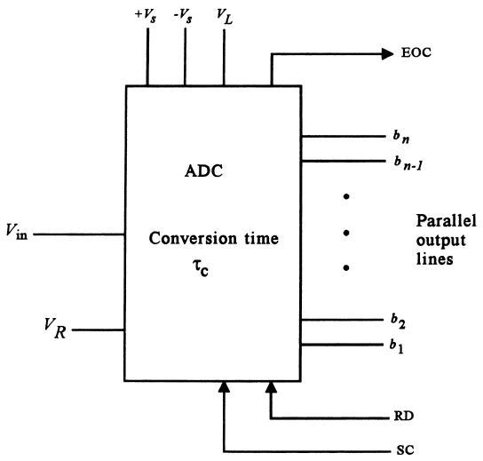
3.3 Analog‑to‑Digital Converters (ADCs): Transfer Function
ADC is the inverse of DAC:
Input: analog voltage \(V_{\text{in}}\) .
Output: \(n\) ‑bit binary word \(b_1 b_2 \dots b_n\) .
Unipolar ADC relationship (reverse of Equation 5):
\[
b_1 2^{-1} + b_2 2^{-2} + \dots + b_n 2^{-n} \;\le\; \frac{V_{\text{in}}}{V_R} \tag{9}
\]
Since the left side can only take discrete values spaced by \(2^{-n}\) :
There is an inherent uncertainty of: \[\Delta V = V_R 2^{-n} \tag{10}\]
Same expression as DAC resolution.
ADC outputs:
All 0’s if \(V_{\text{in}}\) is in the lowest interval.
All 1’s if \(V_{\text{in}}\) is in the highest representable range.
Stress that ADCs quantize the analog value; multiple analog inputs map to the same digital word. Eq. (9) uses ≤ because of truncation: ADC picks the greatest code whose equivalent fraction is still ≤ input fraction.
Designing ADC Resolution: Example 13
Sensor: temperature with \(V = 0.02\ \mathrm{V}/^\circ\mathrm{C} \cdot T\) .
Need to measure from \(0^\circ\mathrm{C}\) to \(100^\circ\mathrm{C}\) with resolution \(0.1^\circ\mathrm{C}\) .
Max sensor output at 100°C:
\[
V_{\max} = 0.02 \cdot 100 = 2\ \mathrm{V}
\]
So choose \(V_R = 2\ \mathrm{V}\) .
Change in sensor voltage for \(0.1^\circ\mathrm{C}\) :
\[
\Delta V_{\text{req}} = 0.1^\circ\mathrm{C} \cdot 0.02\ \mathrm{V}/^\circ\mathrm{C} = 2\ \mathrm{mV}
\]
We need ADC LSB \(\le 2\ \mathrm{mV}\) :
\[
0.002 = 2 \cdot 2^{-n} \Rightarrow 2^{-n} = 0.001 \Rightarrow n \approx 9.996
\]
So 10 bits are required.
Check actual LSB:
\[
\Delta V = 2 \cdot 2^{-10} = 0.001953\ \mathrm{V} \approx 1.95\ \mathrm{mV} < 2\ \mathrm{mV}
\]
Effective temperature range:
Max code (all 1’s) reached at \(V_R(1 - 2^{-n}) \approx 1.998\ \mathrm{V}\) → \(T \approx 99.9^\circ\mathrm{C}\) .
So actual measured range with full 10 bits is about \(0.1^\circ\mathrm{C}\) to \(99.9^\circ\mathrm{C}\) .
Highlight the design thinking: choose reference to match sensor max, then choose bits to meet resolution spec. Note that the effective top of the range is slightly below sensor max output—acceptable in many applications.
Example 14
5‑bit ADC, \(V_R = 5\ \mathrm{V}\) , \(V_{\text{in}} = 3.127\ \mathrm{V}\) .
Compute:
\[
N = \operatorname{INT}\left( \frac{3.127}{5} \cdot 2^5 \right)
= \operatorname{INT}(20.0128) = 20_{10}
\]
Same result as using fractional bits.
Emphasize truncation vs rounding: this is why Eq. (9) uses ≤. Many ADCs behave like this: they map voltage intervals to the lower code boundary; the next code begins at the next threshold.
Example 15: ADC Code & Back‑Conversion
10‑bit ADC, \(V_R = 2.500\ \mathrm{V}\) .
(a) Given \(V_{\text{in}} = 1.45\ \mathrm{V}\) , find hex output.
\[
N = \operatorname{INT}\left(\frac{1.45}{2.5} 2^{10}\right)
= \operatorname{INT}(593.92) = 593_{10}
\]
593₁₀ = 251H.
(b) If output is 1B4H, what \(V_{\text{in}}\) ?
1B4H = 436₁₀. Invert Equation (11):
\[
V_{\text{in}} = \frac{N}{2^n} V_R = \frac{436}{1024} \cdot 2.5 = 1.06445\ \mathrm{V}
\]
But any input in:
\[
[1.06445\ \mathrm{V},\; 1.06445 + \frac{2.5}{1024} = 1.06689\ \mathrm{V})
\]
will quantize to the same code 1B4H.
Every ADC code corresponds to a range of input voltages, not a single unique value.
Highlight that this is why we speak of measurement uncertainty or ±0.5 LSB error even with a perfect (noiseless, linear) ADC.
Bipolar ADC: Offset‑Binary
For bipolar input (e.g., from \(-V_R/2\) to \(+V_R/2\) ), offset‑binary ADC uses:
\[
N = \operatorname{INT}\left[ \left(\frac{V_{\text{in}}}{V_R} + \frac{1}{2} \right) 2^n \right] \tag{12}
\]
Check key points (example: 8‑bit, \(V_R = 10\ \mathrm{V}\) ):
\(V_{\text{in}} = -5.00\ \mathrm{V}\) → \(N = 0\) (00000000₂).\(V_{\text{in}} = 0\) → \(N = 2^{n-1} = 128\) (10000000₂).\(V_{\text{in}} = +5.00\ \mathrm{V}\) not fully representable; max code at ~4.961 V.
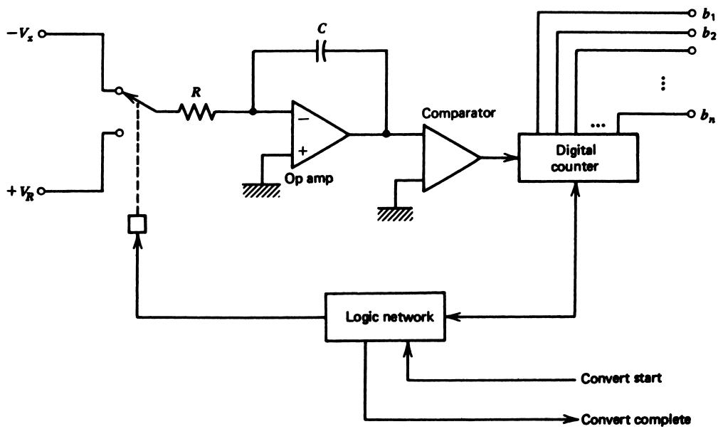
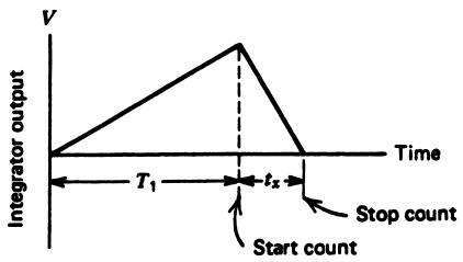
Example 18: Dual‑Slope Conversion Time
Given:
Dual‑slope ADC as in Figure 16.
\(R = 100\ \mathrm{k}\Omega\) , \(C = 0.01\ \mu \mathrm{F}\) \(V_R = 10\ \mathrm{V}\) , \(T_1 = 10\ \mathrm{ms}\) Input \(V_x = 6.8\ \mathrm{V}\) .
Step 1: Compute \(V_1\) :
\[
V_1 = \frac{T_1}{RC} V_x
= \frac{10\ \mathrm{ms}}{(100\ \mathrm{k}\Omega)(0.01\ \mu \mathrm{F})} \cdot 6.8
= 6.8\ \mathrm{V}
\]
(Here, the RC values make the integrator output equal to \(V_x\) after 10 ms.)
Step 2: Compute \(t_x\) using Equation (17):
\[
t_x = \frac{T_1 V_x}{V_R} = \frac{10\ \mathrm{ms} \cdot 6.8}{10} = 6.8\ \mathrm{ms}
\]
Total conversion time:
\[
T_{\text{conv}} = T_1 + t_x = 10\ \mathrm{ms} + 6.8\ \mathrm{ms} = 16.8\ \mathrm{ms}
\]
Point out that this is much slower than SAR but acceptable for many process‑control and DMM applications where signals change slowly.
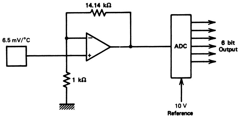
Interfacing Sensors to ADCs: Example 19
Sensor: \(V_T = 6.5\ \mathrm{mV}/^\circ\mathrm{C} \cdot T\) up to 100°C.
6‑bit ADC, \(V_R = 10\ \mathrm{V}\) .
(a) Design amplifier gain so max code at 100°C.
Sensor output at 100°C:
\[
V_{\text{sensor,max}} = 6.5\ \mathrm{mV/^\circ C} \cdot 100^\circ\mathrm{C} = 0.65\ \mathrm{V}
\]
ADC input code 111111₂ → \(V_x\) from Equation (5):
\[
V_x = V_R \left( \frac{1}{2} + \dots + \frac{1}{64} \right)
= 10 \cdot 0.984375 = 9.84375\ \mathrm{V}
\]
Required amplifier gain:
\[
\text{gain} = \frac{9.84375}{0.65} \approx 15.14
\]
Use op‑amp configuration (Figure 18) to implement this gain.
(b) Temperature resolution
ADC LSB:
\[
\Delta V_{\text{ADC}} = V_R 2^{-6} = 10 \cdot 2^{-6} = 0.15625\ \mathrm{V}
\]
Sensor equivalent change at input:
\[
\Delta V_T = \frac{0.15625}{15.14} = 0.01032\ \mathrm{V}
\]
Convert to temperature:
\[
\Delta T = \frac{0.01032\ \mathrm{V}}{6.5\ \mathrm{mV}/^\circ\mathrm{C}} \approx 1.59^\circ\mathrm{C}
\]
Show how amplification improves effective resolution in temperature: instead of wasting ADC range, we scale sensor’s small voltage up to use nearly the full reference.
So:
\[
\omega V_0 \le \frac{V_R}{2^n \tau_c} \Rightarrow
\omega \le \frac{V_R}{2^n \tau_c V_0} \tag{19}
\]
In terms of frequency \(f = \omega/(2\pi)\) :
\[
f \le \frac{V_R}{2^{n+1} \pi \tau_c V_0} \tag{20}
\]
For full‑scale sinusoid \(V_0 = V_R\) :
\[
\omega_{\max} \approx \frac{1}{2^{10} \cdot 20\ \mu\mathrm{s}} \approx 48.8\ \mathrm{rad/s} \Rightarrow f_{\max} \approx 7.8\ \mathrm{Hz}
\]
Even though \(τ_c\) = 20 µs seems fast, for 10‑bit accuracy , the max signal frequency is surprisingly low if we require no 1‑LSB change during conversion.
This is a conceptual wake‑up call. In practice, we use sample‑and‑hold circuits so the input is constant during conversion, relaxing the slew‑rate limitation.
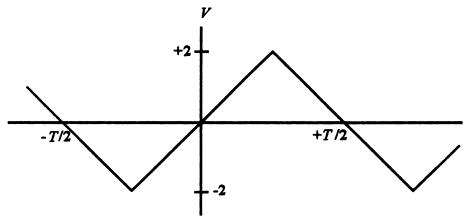
Example 20: Triangular Wave Limit
8‑bit bipolar ADC, \(V_R = 5\ \mathrm{V}\) , \(τ_c = 12\ \mu\mathrm{s}\) .
Input: triangular wave from −1 V to +1 V with period \(T\) (see Figure 19).
Slope of each edge:
Change = 2 V (from −1 V to +1 V) in \(T/4\) : \[
\frac{dV_{\text{in}}}{dt} = \frac{2}{T/4} = \frac{8}{T} = 8f
\]
From Equation (18):
\[
8f \le \frac{5}{2^8 \cdot 12\times10^{-6}} = 1627.6\ \mathrm{V/s}
\]
So:
\[
f \le 203.5\ \mathrm{Hz}
\]
Above this frequency, the ADC cannot maintain 8‑bit accuracy on this triangular wave without a sample‑and‑hold.
Here the slope is bounded not by the amplitude directly but by the waveform shape. This demonstrates a more general approach: evaluate dV/dt for given waveform, then apply Equation (18).
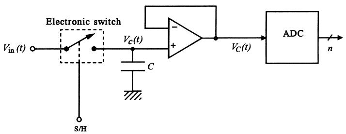
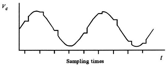
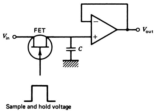
Sample‑and‑Hold (S/H): Concept
Solution to slew‑rate problem: hold the input constant during conversion.
Operation:
Sample mode: switch closed, capacitor \(C\) tracks \(V_{\text{in}}(t)\) → \(V_C \approx V_{\text{in}}(t)\) .At sampling instant \(t_s\) : switch opens → Hold mode.
\(V_C\) “freezes” near \(V_{\text{in}}(t_s)\) .
Buffer (voltage follower) drives ADC input with \(V_C\) while ADC converts.
Show how \(V_C\) becomes a staircase approximation to \(V_{\text{in}}\) . After conversion completes, S/H returns to sample mode, updating the held value at the next sample instant.
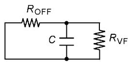
Practical S/H Circuits and Nonidealities
FET used as an electronic switch. Nonideal aspects:
We must choose \(C\) such that droop during conversion doesn’t exceed 1 LSB according to Equation (18). This leads to:
\[
\frac{V_C}{\tau_D} \le \frac{V_R}{2^n \tau_c} \Rightarrow
\tau_D \ge 2^n \tau_c \frac{V_C}{V_R} \tag{24}
\]
Typically evaluate worst case \(V_C = V_R\) .
Clarify that during hold, \(V_C\) decays exponentially. For small hold times, decay is nearly linear and slope ≈ \(V_C/\tau_D\) . We compare that slope to allowed dV/dt from Equation (18).
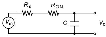
Example 21: Choosing S/H Capacitor
Given:
Unipolar 12‑bit ADC, \(τ_c = 30\ \mu\mathrm{s}\)
S/H parameters: \(R_{\text{ON}} = 10\ \Omega\) , \(R_{\text{OFF}} = 10\ \mathrm{M}\Omega\)
Buffer input resistance \(R_{VF} = 10\ \mathrm{M}\Omega\)
Source resistance \(R_s = 50\ \Omega\)
S/H Timing: Acquisition & Aperture
Important dynamic parameters:
Acquisition time, \(\tau_{\text{acq}}\) : time to charge \(C\) to within 1 LSB of new input when returning to sample mode. Limits how fast we can sample.Aperture time, \(\tau_{\text{ap}}\) : delay between the “hold” command and the actual instant when input is isolated and held. Causes a timing error in effective sampling instant.
Total time between valid samples (throughput):
\[
T = \tau_c + \tau_{\text{acq}} + \tau_{\text{ap}} \tag{25}
\]
Maximum sampling frequency:
\[
f_{\max} = \frac{1}{T}
\]
Example
Given:
\(\tau_{\text{ap}} = 50\ \mathrm{ns}\) \(\tau_{\text{acq}} = 4\ \mu\mathrm{s}\) ADC: \(\tau_c = 40\ \mu\mathrm{s}\)
Then:
\[
T = 40\ \mu\mathrm{s} + 4\ \mu\mathrm{s} + 0.05\ \mu\mathrm{s} = 44.05\ \mu\mathrm{s}
\]
\[
f_{\max} \approx \frac{1}{44.05\ \mu\mathrm{s}} \approx 22.7\ \mathrm{kHz}
\]
Compare this with Nyquist: if you sample at 22.7 kHz, you can represent signals up to ~11 kHz (if other constraints like slew are satisfied).
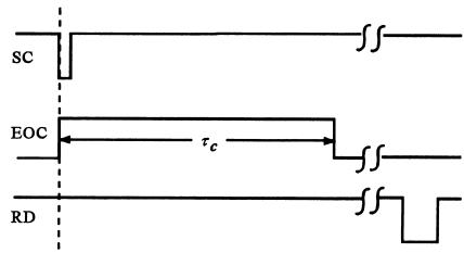
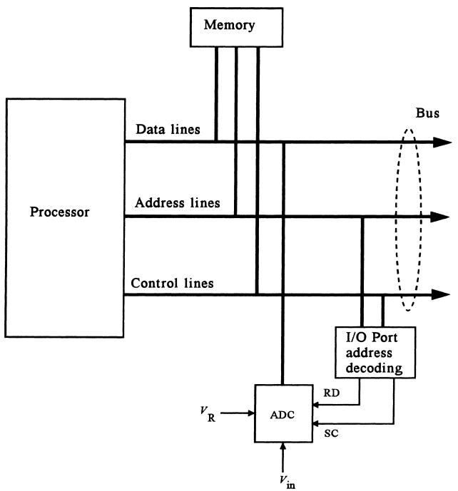
Microprocessor‑Compatible ADCs
Modern ADCs commonly provide:
Tri‑state digital outputs → connect directly to CPU data bus.Control lines mapped into I/O or memory address space .
Microprocessor issues:
Start‑convert by writing to control register/address.
Polls or interrupts on EOC.
Reads data via memory or I/O read.
Address decoder logic determines which addresses correspond to ADC controls/data.
Relate to lab experience: e.g., using SPI ADC where chip‑select and command bytes play similar roles to SC/RD/EOC. The block diagram abstracts bus‑based interfacing.
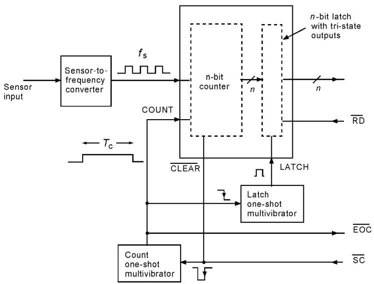
3.4 Frequency‑Based Converters
Another A/D strategy: convert sensor signal into frequency , then count pulses.
Components:
Sensor → V‑to‑F converter : output square wave frequency \(f_s \propto\) sensor signal.
Counter counts pulses over fixed time \(T_c\) .One‑shot (monostable) sets \(T_c\) and then latches count; falling edge = EOC.Computer reads counter value as digital representation of analog input.
For \(n\) ‑bit counter, to use full range at \(f_{\max}\) :
\[
T_c = \frac{2^n - 1}{f_{\max}} \tag{26}
\]
For intermediate frequency \(f\) , count:
\[
N = f T_c
\]
Emphasize advantages: good noise immunity (counting pulses), simple digital hardware. Disadvantage: usually slower than SAR ADCs.
Example 23: 8‑bit Frequency‑Based ADC
Sensor: frequency varies from 2.0 to 20 kHz; use 8‑bit counter.
Max count: \(2^8 - 1 = 255\) .
Design \(T_c\) so that \(f_{\max} = 20\) kHz → N = 255:
\[
T_c = \frac{255}{20,000} = 0.01275\ \mathrm{s} = 12.75\ \mathrm{ms}
\]
At \(f_{\min} = 2.0\) kHz:
\[
N = f_{\min} T_c = 2000 \cdot 0.01275 = 25.5 \Rightarrow 25_{10} = 00011001_2
\]
So digital output ranges from about 25 to 255 over sensor’s frequency range.
Show that resolution is effectively \((255-25)\) counts over the actual signal range—slightly less than full 8‑bit resolution because the sensor never outputs less than 2 kHz.
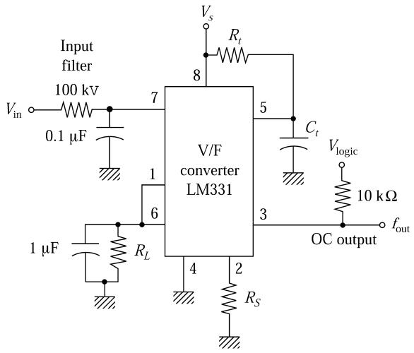
Voltage‑to‑Frequency Conversion: LM331
LM331 output frequency:
\[
f_{\text{out}} = \frac{R_S}{R_L} \frac{1}{R_t C_t} \frac{V_{\text{in}}}{2.09} \tag{27}
\]
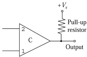
\(R_S \approx 10\) –\(20\ \mathrm{k}\Omega\) (adjust scaling).\(R_L \approx 100\ \mathrm{k}\Omega\) (defines discharge path).\(R_t, C_t\) set nominal frequency range.Output is open‑collector → need pull‑up resistor.
Design example: 0–5 V input → ~0–10 kHz output.
Take \(R_S = 15\ \mathrm{k}\Omega\) , \(R_L = 100\ \mathrm{k}\Omega\) . For \(V_{\text{in,max}} = 5\ \mathrm{V}\) , we want \(f_{\text{out}} = 10\) kHz:
\[
10,000 = \frac{15k}{100k} \frac{1}{R_t C_t} \frac{5}{2.09}
\Rightarrow R_t C_t \approx 3.59 \times 10^{-5}\ \mathrm{s}
\]
Pick \(C_t = 0.01\ \mu\mathrm{F}\) → \(R_t \approx 3.6\ \mathrm{k}\Omega\) .
Highlight that other ICs can convert current, resistance, or capacitance to frequency; LM331 is a classic voltage‑to‑frequency converter. These are especially useful in noisy environments or long‑distance transmission.
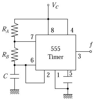
555 Timer as Frequency Sensor Interface
Standard astable frequency:
\[
f = \frac{1}{0.693 (R_A + 2 R_B) C} \tag{28}
\]
If \(R_A\) or \(C\) is a sensor (e.g., light‑dependent resistor, capacitive level sensor), then frequency changes with the measured variable.
Use this frequency with the counter‑based ADC approach from Figure 25.
The 555 is cheap and everywhere. This method is common in low‑cost instrumentation (e.g., light sensors, RC humidity sensors) where precision is moderate and cost/simplicity is important.
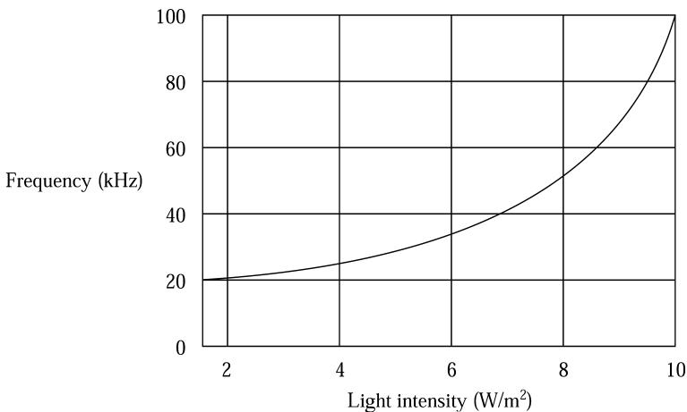
Example 24: Light‑Dependent Resistor to 10‑bit Frequency‑ADC
Sensor: \(R_A\) varies from 36 kΩ at 1.5 W/m² to 4 kΩ at 10 W/m².
Use 555 timer with:
\(R_B = 2\ \mathrm{k}\Omega\) Choose \(C\) and count time \(T_c\) for 10‑bit counter (max 1023).
Let’s choose \(T_c = 10\ \mathrm{ms}\) . Then:
Maximum frequency at \(R_A = 4\ \mathrm{k}\Omega\) should give N ≈ 1023:
\[
f_{\max} = \frac{1023}{T_c} = 102,300\ \mathrm{Hz}
\]
From Equation (28):
\[
102,300 = \frac{1}{0.693 (4k + 2R_B) C}
\]
Pick \(R_B = 2\) kΩ, so \(R_A + 2R_B = 4k + 4k = 8k\Omega\) :
\[
C \approx \frac{1}{0.693 \cdot 8k \cdot 102,300} \approx 0.00018\ \mu\mathrm{F}
\]
At minimum light (1.5 W/m², \(R_A = 36\) kΩ):
\[
f_{\min} = \frac{1}{0.693 (36k + 4k) C} \approx 20,042\ \mathrm{Hz}
\]
Count:
\[
N_{\min} = f_{\min} T_c \approx 200
\]
So digital output varies roughly from 200 to 1023 as light increases. The relationship is nonlinear because \(f \propto 1/(R_A + 2R_B)\) .
Highlight that nonlinearity may be acceptable if we can calibrate via software, or we can linearize using analog pre‑processing. Frequency‑based conversion is flexible but may trade off linearity.
Summary / Key Points
Comparators
1‑bit A/Ds that output high/low based on input vs reference.
Used for alarms, zero‑crossing detection, and inside ADC/DACs.
Noise near threshold causes chattering → fix with hysteresis (Schmitt triggers).
Open‑collector outputs require pull‑ups and allow wired‑OR and level flexibility.
DACs
Unipolar: \(V_{\text{out}} = \frac{N}{2^n} V_R\) .
Bipolar (offset‑binary): \(V_{\text{out}} = \frac{N}{2^n} V_R - V_R/2\) .
Resolution: \(\Delta V = V_R 2^{-n}\) sets smallest output step.
Implemented with R–2R ladders and op‑amps.
ADCs
Quantize input: \(N = \operatorname{INT}(\frac{V_{\text{in}}}{V_R} 2^n)\) .
Resolution/uncertainty same \(\Delta V = V_R 2^{-n}\) .
SAR ADC: fast, medium‑resolution, uses internal DAC + comparator.
Dual‑slope ADC: slow but very accurate and stable; common in DMMs.
Dynamic effects
Converters need finite time to convert → input must be stable during that time.
Input slew‑rate limit: \(\frac{dV_{\text{in}}}{dt} \le \frac{V_R}{2^n \tau_c}\) .
Sample‑and‑Hold circuits freeze input during conversion; design must consider droop, bandwidth, acquisition, and aperture times. Frequency‑based A/D
Sensor → frequency → counter over fixed interval.
Used with V‑to‑F converters (LM331) or 555 timer circuits.
Typically slower; may be nonlinear but robust and simple in some applications.
Encourage students to connect each concept to a real application: alarms with comparators, PWM vs DAC for motor control, selecting ADC resolution for a temperature logger, using S/H in high‑speed DAQ, and using frequency‑based conversion for noisy environments or remote sensors.
DACs
Unipolar DAC output: \[
V_{\text{out}} = V_R \left( b_1 2^{-1} + \dots + b_n 2^{-n}\right) \tag{5}
\] or \[
V_{\text{out}} = \frac{N}{2^n} V_R \tag{6}
\]
Bipolar DAC (offset‑binary): \[
V_{\text{out}} = \frac{N}{2^n} V_R - \frac{1}{2} V_R \tag{7}
\]
DAC / ADC resolution (LSB size): \[
\Delta V = V_R 2^{-n} \tag{8,10}
\]
ADCs
Unipolar ADC inequality: \[
b_1 2^{-1} + \dots + b_n 2^{-n} \le \frac{V_{\text{in}}}{V_R} \tag{9}
\]
Unipolar ADC code: \[
N = \operatorname{INT}\left(\frac{V_{\text{in}}}{V_R} 2^n\right) \tag{11}
\]
Bipolar ADC (offset‑binary): \[
N = \operatorname{INT}\left[\left(\frac{V_{\text{in}}}{V_R} + \frac{1}{2}\right) 2^n\right] \tag{12}
\]
Dual‑Slope ADC
Integrator output after input phase: \[
V_1 = \frac{T_1}{RC} V_x \tag{14}
\]
Voltage during reference discharge: \[
V_2 = \frac{T_1}{RC} V_x - \frac{t_x}{RC} V_R \tag{16}
\]
Relation between input and discharge time: \[
V_x = \frac{t_x}{T_1} V_R \tag{17}
\]
Dynamic Constraints & S/H
Max allowed input slew during conversion: \[
\frac{dV_{\text{in}}}{dt} \le \frac{V_R}{2^n \tau_c} \tag{18}
\]
For sinusoid \(V_{\text{in}} = V_0 \sin(\omega t)\) : \[
\omega \le \frac{V_R}{2^n \tau_c V_0} \tag{19}
\] \[
f \le \frac{V_R}{2^{n+1} \pi \tau_c V_0} \tag{20}
\]
S/H sampling cutoff: \[
f_c = \frac{1}{2\pi (R_s + R_{\text{ON}}) C} \tag{21}
\]
Droop time constant: \[
\tau_D = \frac{R_{\text{OFF}} R_{VF}}{R_{\text{OFF}} + R_{VF}} C \tag{22}
\]
Droop constraint: \[
\tau_D \ge 2^n \tau_c \frac{V_C}{V_R} \tag{24}
\]
Sampling throughput: \[
f_{\max} = \frac{1}{\tau_c + \tau_{\text{acq}} + \tau_{\text{ap}}} \tag{25}
\]
Frequency‑Based Converters
Count time for \(n\) ‑bit counter with max frequency \(f_{\max}\) : \[
T_c = \frac{2^n - 1}{f_{\max}} \tag{26}
\]
Count for arbitrary frequency \(f\) : \[
N = f T_c
\]
LM331 V‑to‑F converter (approx): \[
f_{\text{out}} = \frac{R_S}{R_L} \frac{1}{R_t C_t} \frac{V_{\text{in}}}{2.09} \tag{27}
\]
555 timer astable frequency: \[
f = \frac{1}{0.693 (R_A + 2 R_B) C} \tag{28}
\]
Encourage students to keep this formula summary handy for homework and labs. Many instrumentation design tasks reduce to plugging realistic numbers into these equations, then checking if performance (resolution, speed, range) meets specs.
How Many Bits Do You Need? (DAC/ADC Resolution Explorer)
Use this interactive cell to explore how reference voltage and number of bits affect the LSB size (resolution) for DACs and ADCs using
\[\Delta V = V_R 2^{-n}\]
Ask students to: - Double \(n\) (e.g., from 8 to 16) and see what happens to \(\Delta V\) . - Change \(V_R\) and see how the same number of bits yields different absolute resolutions. Connect results to the examples in the main slides (e.g., 10‑bit, 10 V reference).
DAC Output Calculator (Unipolar)
Experiment with converting a digital code to an analog voltage using
\[V_{\text{out}} = \dfrac{N}{2^n} V_R\]
Prompt students to: - Try \(N = 0\) , \(N = 2^n - 1\) , and some mid‑range codes. - Relate \(N = 255\) and \(V_R = 5\) to the example that produced 3.2617 V for A7H. - Notice that \(V_{\max}\) is slightly less than \(V_R\) because \(N \le 2^n-1\) .
ADC Output Code Calculator (Unipolar)
Now convert analog voltage to digital code using
\[
N = \operatorname{INT}\left(\frac{V_{\text{in}}}{V_R} 2^n\right)
\]
Ask: - What happens if \(V_{\text{in}} > V_R\) or \(V_{\text{in}} < 0\) ? - Compare with Example 15: note that 1.45 V gives 251H for \(V_R = 2.5\) , \(n = 10\) . - Discuss why INT (truncate) is used rather than rounding.
Bipolar DAC Explorer (Offset‑Binary)
Explore a bipolar DAC :
\[
V_{\text{out}} = \frac{N}{2^n} V_R - \frac{1}{2} V_R
\]
Students can try: - \(N = 0\) → near \(-V_R/2\) . - \(N = 2^{n-1}\) → near 0 V. - Large \(N\) near \(2^n-1\) → just below \(+V_R/2\) . Connect back to Example 10 and the bipolar DAC discussion.
Comparator with Hysteresis – Threshold Explorer
Use this cell to experiment with hysteresis width \(\Delta V\) for a comparator:
\[
\Delta V = \frac{R}{R_f} V_0
\]
Relate values to the tank splashing example (R_f = 100 kΩ, R = 3 kΩ). Encourage students to answer: - How large must R/R_f be to tolerate ±60 mV noise? - What happens to ΔV when they halve/double R?
Reactive Demo 1 – Interactive DAC Transfer (OJS + Pyodide + Plotly)
Use the sliders to control number of bits and reference voltage . The DAC transfer curve updates in real time.
= Inputs. range ([2 , 12 ], {step : 1 , label : "Number of bits (n)" })= Inputs. range ([1 , 10 ], {step : 0.5 , label : "Reference voltage V_R (V)" })
Guide students to: - Observe how increasing bits increases the number of steps and decreases step height. - Compare LSB visually as \(n\) changes. - Relate to physical actuator control (e.g., how “smooth” a valve position looks).
Reactive Demo 2 – ADC Quantization of a Ramp Signal
Visualize how an ADC with given n and V_R quantizes a linearly increasing input.
= Inputs. range ([3 , 12 ], {step : 1 , label : "ADC bits (n)" })= Inputs. range ([1 , 10 ], {step : 0.5 , label : "ADC reference V_R (V)" })
Discussion prompts: - Identify the step size from the plot and compare to \(\Delta V = V_R 2^{-n}\) . - Look at what happens to low vs high resolution (3 bits vs 12 bits). - Relate the stepped curve to codes like those computed in Examples 14–15.
Reactive Demo 3 – Successive Approximation (4‑bit)
Simulate the successive approximation process for a 4‑bit ADC with \(V_R = 5\ \mathrm{V}\) , as in Example 17.
= Inputs. range ([0 , 5 ], {step : 0.05 , label : "Input voltage V_x (V)" })
Students can adjust \(V_x\) and observe how the algorithm sets/reset bits. Relate directly to Example 17 with \(V_x = 3.217\ \mathrm{V}\) . Emphasize binary search nature and constant conversion time in steps of \(n\) .
Reactive Demo 4 – Slew Rate Limit vs Conversion Time
Explore Equation (18):
\[
\frac{dV_{\text{in}}}{dt} \le \frac{V_R}{2^n \tau_c}
\]
= Inputs. range ([4 , 16 ], {step : 1 , label : "ADC bits n" })= Inputs. range ([1 , 10 ], {step : 0.5 , label : "Reference V_R (V)" })= Inputs. range ([1 , 100 ], {step : 1 , label : "Conversion time τ_c (µs)" })
Have students see how: - Increasing bits or conversion time tightens the allowable dV/dt. - This motivates sample‑and‑hold circuits to freeze the input during conversion.
Reactive Demo 5 – Frequency‑Based ADC (Counter Method)
Explore the counter‑based A/D relationship for an \(n\) ‑bit counter and a signal frequency \(f\) .
Given
\[T_c = \frac{2^n - 1}{f_{\max}}, \quad N = f T_c\]
= Inputs. range ([4 , 12 ], {step : 1 , label : "Counter bits n" })= Inputs. range ([1 , 100 ], {step : 1 , label : "Max sensor frequency f_max (kHz)" })= Inputs. range ([0.1 , 100 ], {step : 0.1 , label : "Current sensor frequency f (kHz)" })
Connect this to Example 23 and Example 24: - See how count saturates at \(2^n - 1\) when \(f = f_{\max}\) . - Encourage students to pick realistic ranges (e.g., 2–20 kHz) and relate to the text.