For typical values (\(A=200{,}000\), \(z_0=75\Omega\), \(z_{\text{in}}=2\text{M}\Omega\), \(R_2/R_1=100\)), we get \(\mu \approx 0.0005\), so the error in gain is about \(0.05\%\).
Note
Conclusion: for low‑frequency instrumentation work and reasonable resistor values, ideal op amp analysis is usually accurate enough.
Op Amp Data Sheet Specifications
Beyond \(A\), \(z_{\text{in}}\), \(z_0\), several key specs matter in practice:
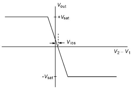
Input offset voltage \(V_{\text{ios}}\)
Small input differential required to force \(V_{\text{out}}=0\).
Results in small DC error at output even when input is zero.
Input bias currents \(I_{B+}, I_{B-}\)
Average current needed into each input to bias internal transistors.
Input offset current
Difference between the two input bias currents.
Slew rate (SR)
Maximum rate of change of output voltage (V/μs) for large‑signal steps.
Limits how fast output can move ⇒ important for fast signals.
Unity‑gain bandwidth (gain–bandwidth product)
Frequency where open‑loop gain falls to 1.
For closed‑loop gain \(G\), approximate bandwidth \(\approx \frac{f_T}{G}\).
These can all show up as accuracy, drift, or speed limitations in instrumentation circuits.
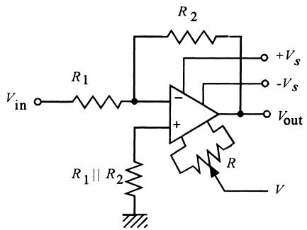
Practical Power & Offset Compensation
Op amp powered by bipolar supplies: typically \(\pm 9\) to \(\pm 15\ \text{V}\) in classical designs.
Many packages offer pins for offset‑null:
Use a small trimmer pot between these pins and a supply.
Adjust until output is 0 V when input is 0 V ⇒ cancel \(V_{\text{ios}}\).
Offset current compensation trick:
Make the resistance seen by + input equal to the Thevenin resistance seen by − input.
That way, both bias currents produce similar drops → smaller output error.
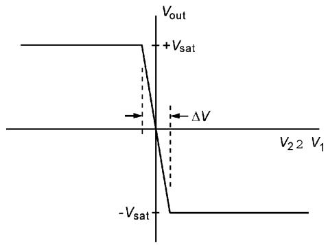
Inverting amplifier with power & offset trim
Design Rule of Thumb: “Think mA and kΩ”
Most general‑purpose op amps can source/sink only tens of mA.
Avoid tiny resistors that force huge currents.
Example (text Example 17):
Want gain \(-4.5\).
Mathematically, you could pick \(R_1=1\Omega\), \(R_2=4.5\Omega\).
If \(V_{\text{in}}=2\ \text{V}\) ⇒ \(V_{\text{out}}=-9\ \text{V}\).
Feedback current \(I_2 = (-9\text{V})/4.5\Omega = -2\ \text{A}\) ⇒ impossible.
Larger CMRR ⇒ better rejection of noise or interference that appears on both inputs.
Typical CMR values: \(60\)–\(100\ \text{dB}\).
Instrumentation use case: bridge outputs a few mV difference sitting on several volts of common‑mode bias. A good differential/instrumentation amplifier extracts the tiny difference accurately.
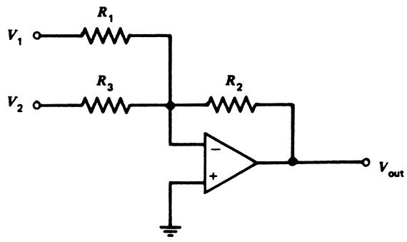
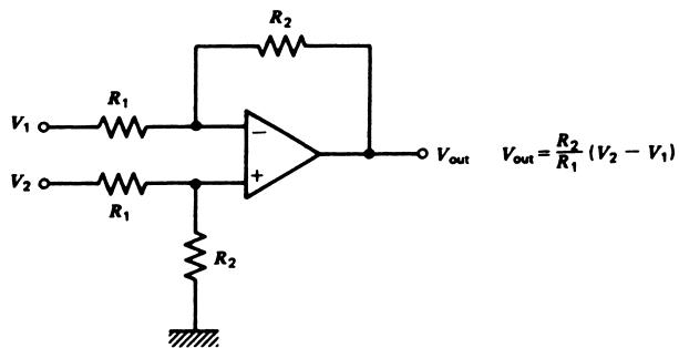
Basic Differential Amplifier Circuit
Differential amplifier
Using carefully matched resistors (\(R_1\) pair, \(R_2\) pair):
\[
V_{\text{out}} = \frac{R_2}{R_1}(V_2 - V_1)
\]
Same gain for both inputs (but one inverted).
CMR performance is very sensitive to resistor matching.
Limitations:
Input impedance is only on the order of \(R_1\) for each input.
Not well suited to very high‑impedance sensors.
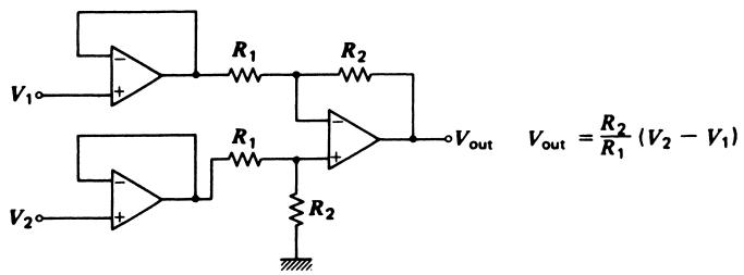
Instrumentation Amplifier (3‑Op‑Amp Version)
Instrumentation amplifier with followers
Add voltage followers (or gain‑blocks) in front of the differential stage.
Pros:
Very high input impedance.
Low output impedance.
Transfer function stays: \[
V_{\text{out}} = \frac{R_2}{R_1}(V_2 - V_1)
\]
Gain adjustment may require changing two resistors in the differential stage.
Many ICs integrate all three op amps plus trimmed resistors into a single instrumentation‑amplifier package.
Popular 3‑Op‑Amp Instrumentation Amplifier Topology
Goal: 0–1 V input → 0–10 mA output, op amp saturates at ±10 V.
V–I converter inverts (\(I\propto -V_{\text{in}}\)), so use a first‑stage inverting amplifier to produce \(0\) to \(-1\ \text{V}\) from the original \(0\) to \(1\ \text{V}\).
In V–I stage of Figure 39, choose \(R_1=R_2\) ⇒ \[
I = \frac{V_{\text{in}}}{R_3}
\]
For \(I_{\max}=10\ \text{mA}\) at \(|V_{\text{in}}|=1\ \text{V}\): \[
R_3 = \frac{1\ \text{V}}{10\ \text{mA}} = 100\ \Omega
\]
Let \(R_5=0\) ⇒ from \(R_1(R_3 + R_5) = R_2 R_4\) and \(R_1=R_2\): \[
R_4 = R_3 = 100\ \Omega
\]
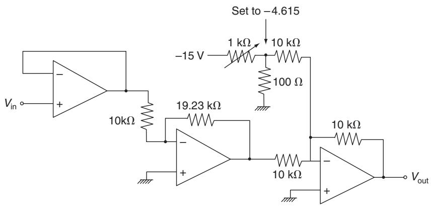
Use an inverting amplifier with \(R_s\) in feedback, plus a fixed input voltage to generate a term proportional to \(R_s\).
Follow with a summing inverter to add the constant bias −8.58 V and correct the sign.
Set the fixed input resistor and voltage so sensor current stays ≤ 1 mA (safely under 2 mA).
One possible solution for Example 25
The 1 V / 1 kΩ source guarantees 1 mA through Rs.
Trimmers allow precise adjustment of the 1.00 V and 8.58 V reference levels.
Summary / Key Points
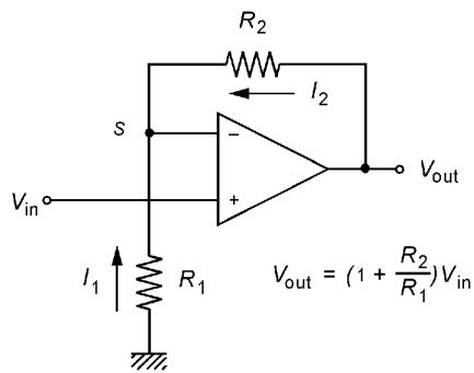
Op amp basics: treat the op amp as a high‑gain differential amplifier; with feedback, we can assume \(V_{+}=V_{-}\) and no input current for ideal analysis.
Core configurations:
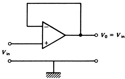
Voltage follower: unity gain, very high input Z, low output Z.
Inverting amplifier: gain \(-R_2/R_1\), input Z ≈ \(R_1\).
Noninverting amplifier: gain \(1+R_2/R_1\), very high input Z.
Summing amplifier: weighted sum of inputs.
Differential and instrumentation amplifiers:
Extract small differences (\(V_a - V_b\)) in presence of large common‑mode voltage.
CMR/CMRR key metrics; resistor matching critical.
3‑op‑amp instrumentation amps provide high Z, adjustable gain via \(R_G\).
Process control interfaces:
Voltage–current converter to generate 4–20 mA‑type signals.
Design an inverting amplifier with gain −10 and input impedance ≥ 20 kΩ. Specify \(R_1, R_2\).
For a 4–20 mA current loop, choose \(R\) in a current‑to‑voltage converter so that the output spans 1–5 V.
You have a strain‑gauge bridge producing −10 to +10 mV. Design a front‑end instrumentation amplifier to produce −5 to +5 V. Estimate required gain and discuss CMRR needs.
Operational Amplifiers in Instrumentation - Interactive
Use this sandbox to see how changing \(R_1\), \(R_2\), or \(V_{\text{in}}\) alters the output.
Try:
Make \(R_2 < R_1\). What happens to \(|V_{\text{out}}|\) relative to \(|V_{\text{in}}|\)?
Make \(R_2 \gg R_1\). How large can \(V_{\text{out}}\) get before it would hit typical \(V_{\text{sat}}\) (e.g., ±10 V)?
2. Practical Design Rule: “Think mA and kΩ”
We rarely want currents above tens of mA in op amp circuits. This cell computes the feedback current in an inverting amplifier and warns if it is too high.
Consider the bridge of Example 21, with \(R_4\) varying from 100 to 102 Ω, and supply 5 V. An instrumentation amplifier with gain \(A_d \approx 101\) converts the small \(\Delta V\) into a 0–2.5 V signal.
This interactive cell lets you vary \(R_4\) and \(R_G\) and see the resulting \(V_{\text{out}}\).
viewof R4_ohms = Inputs.range([100,102], {step:0.01,label:"R4 (Ω) in bridge"})viewof RG_ohms_bridge = Inputs.range([1_000,5_000], {step:100,label:"RG (Ω) in instrumentation amp"})
Try:
Set \(R_4=100\ \Omega\) (bridge balanced). What is \(V_{\text{out}}\)?
Set \(R_4=102\ \Omega\) and tune \(R_G\) so that \(V_{\text{out}} \approx 2.5\ \text{V}\).