Analog Signal Conditioning
Instrumentation 2.1
Learning Objectives
By the end of this session, you should be able to:
Explain the role of analog signal conditioning in a measurement / control system.
Describe and apply basic signal-level changes : biasing, amplification, attenuation.
Explain loading using Thévenin models and compute its effect on measurements.
Use voltage dividers and bridge circuits to convert resistance/impedance changes into voltages.
Analyze RC filters (low-pass, high-pass, band-pass, notch) and design simple filters for noise reduction.
Connect these concepts to real ECE applications : sensors, ADC interfaces, and industrial 4–20 mA loops.
Emphasize that this lecture is about the “plumbing” between sensors and the rest of the system. Students often jump to digital / microcontroller code and ignore the analog front end, which is where many real‑world problems show up.
1. What Is Analog Signal Conditioning?
Operations on analog signals to convert them into a form suitable for:
Other analog circuits (amplifiers, filters, actuators).
ADC inputs in mixed‑signal systems.
In this chapter, we focus on analog transformations (output still analog).
Even if the final processing is digital, analog conditioning almost always happens first .
Real ECE examples:
ECG front‑end: microvolt cardiac signals → 1–3 V, filtered, centered, then digitized.
Strain gauge bridge on a load cell → mV → amplified / filtered → 4–20 mA transmitter.
Light sensor (CdS cell) → resistance change → voltage via divider/bridge → linearized / scaled for an ADC.
Point out that students see this in lab whenever they need to scale a sensor to an Arduino’s 0–5 V analog input. Stress that this is not “extra stuff”—it’s what determines measurement accuracy and robustness.
2. Principles of Analog Signal Conditioning
2.1 Sensors & Transfer Functions
A sensor / transducer converts a physical variable into an electrical quantity:
Voltage, current, resistance, capacitance, inductance, or frequency.
The relationship between input (physical) and output (electrical) is its transfer function .
Example:
Cadmium sulfide (CdS) photoresistor:
Resistance \(R_{\text{CdS}}\) varies nonlinearly and inversely with light intensity.
We don’t get to choose this curve; nature chose it.
A signal conditioning block also has a transfer function, e.g.
Simple voltage amplifier: \(V_{\text{out}} = K V_{\text{in}}\) (gain \(K\) ).
When you design a measurement system, you are really designing the overall transfer function from physical variable → final electrical (or digital) output.
Stress the idea of transfer functions as “input–output relationships.” Students often see them only in Laplace / systems courses, but here it’s simpler: slope, linear vs. nonlinear, etc.
2.2 Linearization
Figure 1: Linearization concept. (a) Nonlinear sensor output vs variable. (b) Block diagram of linearizer. (c) Resulting linear output vs variable.
Many sensors are nonlinear : \(V_{\text{sensor}}(x)\) vs \(x\) is curved.
But most ADCs / controllers assume a linear mapping between measured variable and digital value.
2.3 Conversions (R→V, V→I, Analog→Digital)
Common conversion tasks in instrumentation:
Resistance change → voltage
Using voltage dividers or bridges (covered later).
Voltage → current (V‑to‑I converter) for transmission.Current → voltage (I‑to‑V converter) at receiver.Analog → Digital (ADC input scaling).
4–20 mA current loop
Industrial standard: transmit measurement as 4–20 mA current.
Why current?
Immune to series resistance: voltage drops along long cables don’t change current (much).
4 mA “live zero” distinguishes broken wire (0 mA).
Need:
At transmitter : convert sensor R or V to 4–20 mA.
At receiver : convert 4–20 mA to voltage, typically via a precision shunt resistor.
Analog to Digital Interface
ADC input may require, e.g. 0–5 V, 0–3.3 V, ±2.5 V, etc.
Sensor might yield 30–80 mV, or a resistance.
Analog conditioning:
Gain + offset + possibly filtering.
Ensure sensor output fully uses ADC input range → better resolution.
Make this concrete with: - 4–20 mA loop driving a 250 Ω resistor → 1–5 V input. - Show quick mental calculation: 20 mA × 250 Ω = 5 V.
2.4 Filtering and Impedance Matching
Filtering
Real environments have noise :
50/60 Hz line interference.
Motor start transients, switching spikes.
High‑frequency EMI from radios, inverters, etc.
Use filters to:
Pass desired band of frequencies.
Reject low / high / narrow‑band noise.
Types (passive or active):
Low-pass : pass low f, block high f (e.g., DC sensor + 60 Hz noise).High-pass : pass high f, block low f (e.g., remove DC offset / drift).Band-pass : pass midband (e.g., audio channel).Band-reject / notch : reject narrow band (e.g., 60 Hz notch).
Impedance Matching
If sensor or line impedance is not matched to the receiving circuit:
You get loading → amplitude errors.
Possible reflections (at high frequency / transmission lines).
Use passive or active networks to:
Present high input impedance to the sensor.
Provide low output impedance to whatever you drive.
Connect this to their previous circuits course: source/load model, maximum power transfer vs. measurement accuracy. Here, we usually care about small loading , not max power.
2.5 Concept of Loading
Any two‑terminal source can be modeled (Thévenin) as:
Ideal voltage source \(V_x\) in series with internal resistance \(R_x\) .
When open‑circuit (no load): output voltage = \(V_x\) .
When you connect a load \(R_L\) :
Current flows, some voltage drops across \(R_x\) .
Loaded output voltage:
\[
V_y = V_x\left(1 - \frac{R_x}{R_L + R_x}\right)
\]
If \(R_L\) is not >> \(R_x\) , \(V_y\) is significantly < \(V_x\) .
Goal in measurement systems: make \(R_L \gg R_x\) to minimize loading.
Loading changes the apparent transfer function of your sensor + conditioning block. If your measurement depends on amplitude , loading matters a lot.
Remind them: in frequency or digital (0/1) detection, exact amplitude may not matter, but for analog magnitude (temperature, pressure), it does.
Example 1 — Loading Between Sensor and Amplifier
Given:
Amplifier gain \(= 10\) , input resistance \(R_L = 10\ \text{k}\Omega\) .
Sensor transfer function: \(20\ \text{mV}/^\circ\text{C}\) , output resistance \(R_x = 5.0\ \text{k}\Omega\) .
Temperature \(T = 50^\circ\text{C}\) .
Naive (no loading) answer:
Sensor open‑circuit: \(V_T = (20\ \text{mV}/^\circ\text{C})(50^\circ\text{C}) = 1.0\ \text{V}\) .
Amplifier output: \(V_{\text{out}} = 10\cdot 1.0\ \text{V} = 10\ \text{V}\) .
Correct answer (include loading):
Sensor and amplifier form a divider:
\[
V_{\text{in}}
= V_T\left(1 - \frac{R_x}{R_x + R_L}\right)
= 1.0\text{ V}\left(1 - \frac{5.0\text{ k}\Omega}{5.0\text{ k}\Omega + 10\text{ k}\Omega}\right)
\]
Numerically: \(V_{\text{in}} \approx 0.67\ \text{V}\) .
Amplifier output: \(V_{\text{out}} = 10 \cdot 0.67\ \text{V} = 6.7\ \text{V}\) .
Error from ignoring loading: \(10\ \text{V}\) vs \(6.7\ \text{V}\) → 33% error.
Use this as a wake‑up example: 33% error is huge. Ask students to think: how could we reduce it? (Increase amplifier input resistance; use a buffer amplifier).
3. Passive Circuits in Signal Conditioning
Two essential passive building blocks:
Voltage dividers .Bridge circuits (Wheatstone, AC bridges).
RC networks used for filtering .
Even though op‑amps are cheap, passive circuits still matter:
High accuracy (e.g., precision bridges).
Simple, low‑power, and often very low noise .
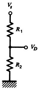
3.1 Voltage Divider Circuits
Two resistors, \(R_1\) and \(R_2\) , in series across supply \(V_s\) .
Output is taken across \(R_2\) .
Divider equation:
\[
V_D = \frac{R_2}{R_1 + R_2} V_s
\tag{2}
\]
Often, either \(R_1\) or \(R_2\) is the sensor whose resistance varies with the measured variable.
Example 2 — Divider with Variable Sensor Resistance
Given (Figure 4):
\(R_1 = 10.0\ \text{k}\Omega\) , \(V_s = 5.00\ \text{V}\) .\(R_2\) is a sensor varying from \(4.00\ \text{k}\Omega\) to \(12.0\ \text{k}\Omega\) .
(a) Range of \(V_D\)
Use Equation (2).
For \(R_2 = 4\ \text{k}\Omega\) :
\[
V_D = \frac{(5\ \text{V})(4\ \text{k}\Omega)}{10\ \text{k}\Omega + 4\ \text{k}\Omega} = 1.43\ \text{V}
\]
For \(R_2 = 12\ \text{k}\Omega\) :
\[
V_D = \frac{(5\ \text{V})(12\ \text{k}\Omega)}{10\ \text{k}\Omega + 12\ \text{k}\Omega} = 2.73\ \text{V}
\]
So \(V_D\) ranges from 1.43 V to 2.73 V.
(b) Output impedance range
\(Z_{\text{out}} = R_1 \parallel R_2\) .
For \(R_2 = 4\ \text{k}\Omega\) : \(Z_{\text{out}} = 2.86\ \text{k}\Omega\) .
For \(R_2 = 12\ \text{k}\Omega\) : \(Z_{\text{out}} = 5.45\ \text{k}\Omega\) .
(c) Power dissipated in \(R_2\)
Use \(P = V_D^2 / R_2\) :
At 4 kΩ: \(P \approx 0.51\ \text{mW}\) .
At 12 kΩ: \(P \approx 0.62\ \text{mW}\) .
Point out: divider output is only ~1.4–2.7 V from 5 V supply → not using full dynamic range. Later you can mention: we may want to add gain to map this to 0–5 V for ADC usage.
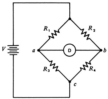
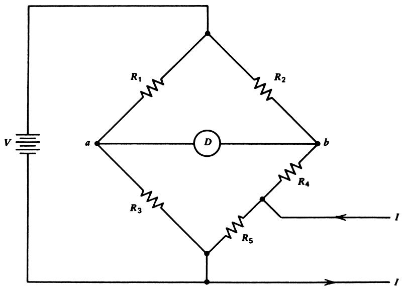
3.2 Wheatstone Bridge Circuits
Purpose : convert small resistance changes into measurable voltage changes.Very commonly used with:
Strain gauges, RTDs, pressure sensors, etc.
Arrangement: four resistors in a diamond, excited by a voltage \(V\) .
Detector \(D\) senses voltage difference between points \(a\) and \(b\) .
Define:
\(V_a =\) potential at node \(a\) w.r.t. node \(c\) .\(V_b =\) potential at node \(b\) w.r.t. node \(c\) .Offset: \(\Delta V = V_a - V_b\) .
Assuming infinite detector impedance (no current through D):
\[
V_a = \frac{V R_3}{R_1 + R_3}
\tag{4}
\]
\[
V_b = \frac{V R_4}{R_2 + R_4}
\tag{5}
\]
So
\[
\Delta V = V_a - V_b
= V\frac{R_3R_2 - R_1R_4}{(R_1 + R_3)(R_2 + R_4)}
\tag{7}
\]
Null (balanced bridge):
When \(\Delta V = 0\) , condition is:
\[
R_3 R_2 = R_1 R_4
\tag{8}
\]
Key advantage: null condition is independent of supply voltage \(V\) .
Show that in many sensors, one or more arms are active (change with variable); others are fixed or used for temperature compensation.
Example 3 — Finding an Unknown Resistance from Bridge Null
Given:
Bridge nulls (ΔV = 0) with \(R_1 = 1000\ \Omega\) , \(R_2 = 842\ \Omega\) , \(R_3 = 500\ \Omega\) .
Find \(R_4\) .
Use Equation (8):
\[
R_1 R_4 = R_3 R_2
\Rightarrow
R_4 = \frac{R_3R_2}{R_1}
= \frac{(500\ \Omega)(842\ \Omega)}{1000\ \Omega}
= 421\ \Omega
\]
So the unknown resistance is 421 Ω.
This is essentially how precise ohmmeters using bridges worked historically. Now replaced by more integrated circuitry but the principle is the same.
Example 4 — Small Offset from Nearly Balanced Bridge
Given:
\(R_1 = R_2 = R_3 = 120\ \Omega\) , \(R_4 = 121\ \Omega\) , \(V = 10.0\ \text{V}\) .Find voltage offset ΔV.
Using Equation (7):
\[
\Delta V
= 10\ \text{V}\cdot
\frac{(120\ \Omega)(120\ \Omega) - (120\ \Omega)(121\ \Omega)}
{(120\ \Omega + 120\ \Omega)(120\ \Omega + 121\ \Omega)}
\]
Result:
\[
\Delta V = -20.7\ \text{mV}
\]
Negative sign → \(V_b > V_a\) .
Highlight sensitivity: 1 Ω change (out of 120 Ω) in one resistor yields ~20 mV offset. With an amplifier, we can detect very small resistance changes.
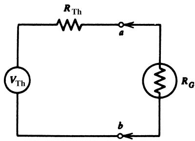
Bridges with Galvanometer Detectors (Finite Detector Resistance)
If the detector is a galvanometer or any finite resistance \(R_G\) :
We replace bridge (between nodes \(a\) and \(b\) ) by its Thévenin equivalent:
Thévenin voltage \(V_{\text{Th}}\) (open‑circuit ΔV).
Thévenin resistance \(R_{\text{Th}}\) .
From earlier:
\[
V_{\text{Th}} = V\frac{R_3R_2 - R_1R_4}{(R_1 + R_3)(R_2 + R_4)}
\tag{9}
\]
Thévenin resistance between \(a\) and \(b\) :
\[
R_{\text{Th}} = \frac{R_1R_3}{R_1 + R_3} + \frac{R_2R_4}{R_2 + R_4}
\tag{10}
\]
Detector current:
\[
I_G = \frac{V_{\text{Th}}}{R_{\text{Th}} + R_G}
\tag{11}
\]
Bridge null condition is still Equation (8).
This is more historical but useful because the same math applies if D is, say, a low‑input‑impedance amplifier; you must then consider loading of the bridge arms.
Bridge Resolution
Detector resolution (minimum measurable ΔV or ΔI) translates to minimum detectable resistance change in the bridge.For high‑input‑impedance detector (e.g., DVM): use Equation (7) or (6) and solve for \(\Delta R\) such that \(\Delta V\) equals detector resolution.
Example 6 — Smallest Measurable Resistance Change
Given:
Bridge: \(R_1 = R_2 = R_3 = R_4 = 120.0\ \Omega\) , \(V = 10.0\ \text{V}\) .
Detector: 3½‑digit DVM on 200 mV range → resolution = \(0.1\ \text{mV} = 100\ \mu\text{V}\) .
Find resolution (smallest \(\Delta R_4\) ) for measurement of \(R_4\) .
Approach:
Bridge is initially nulled (ΔV = 0) when all resistors are 120 Ω.
Now assume \(R_4\) changes to some value giving ΔV = 100 μV.
Use Equation (6) with unknown \(R_4\) and solve.
Result:
\(R_4 = 119.9952\ \Omega\) .\(\Delta R_4 = 120.0000 - 119.9952 = 0.0048\ \Omega\) .
So resolution: about \(4.8\ \text{m}\Omega\) .
Resolution here also tells you the measurement uncertainty (best‑case) using this bridge and detector.
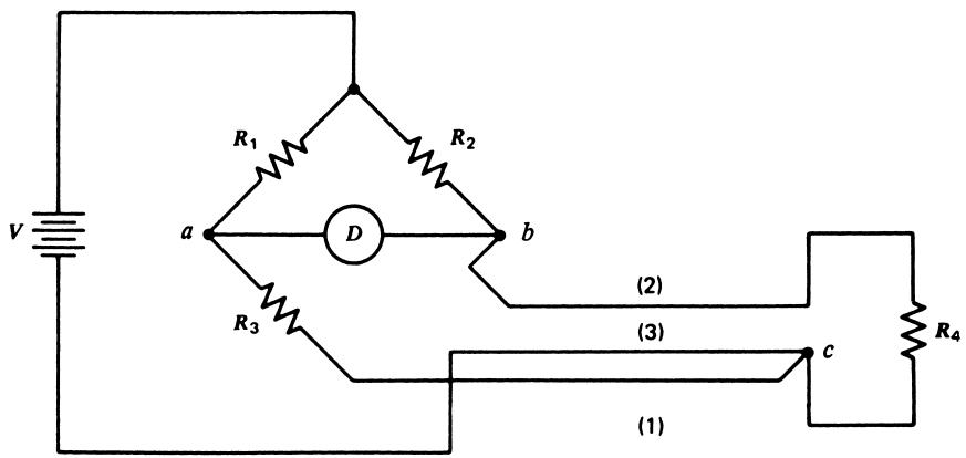
Lead Compensation in Bridges
When sensor \(R_4\) is remotely located, long wires add resistance and can vary with:
Temperature.
Mechanical stress.
Corrosion / chemical vapors.
Lead compensation idea:
Route the wiring so that lead resistance changes are mirrored in two arms (\(R_3\) and \(R_4\) ) of the bridge.
If both arms change by same amount, condition \(R_3R_2 = R_1R_4\) still holds → no change in ΔV.
ECE analogy: 3‑wire RTD configuration widely used in industrial temperature measurement.
Clarify that wire (3) in the figure is just a supply lead, so changes in its resistance don’t affect the bridge balance.
Current-Balance Bridge
Motivation:
Mechanical feedback (motors adjusting resistors) is slow and noisy.
Better to electronically null the bridge using a current source.
Construction:
Split one arm into \(R_4\) and \(R_5\) .
Inject current \(I\) at their junction (into \(R_5\) mostly).
Under conditions \(R_4 \gg R_5\) or \((R_2 + R_4) \gg R_5\) :
\[
V_b = \frac{V(R_4 + R_5)}{R_2 + R_4 + R_5} + I R_5
\tag{14}
\]
Voltage at \(a\) : still Equation (4).
Bridge offset:
\[
\Delta V = V_a - V_b
= \frac{V R_3}{R_1 + R_3} - \frac{V(R_4 + R_5)}{R_2 + R_4 + R_5} - I R_5
\tag{15}
\]
To null the bridge: adjust \(I\) so that \(\Delta V = 0\) .
This is conceptually similar to DAC or feedback current that “balances” an analog bridge — useful in self‑balancing instrumentation.
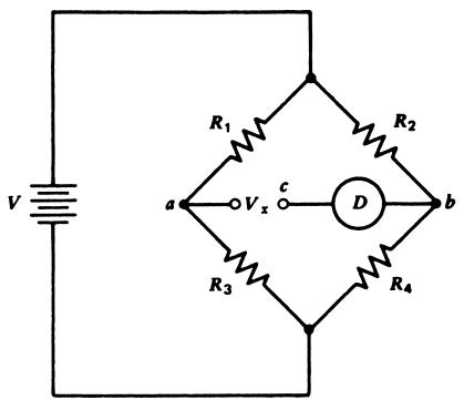
Bridges for Potential Measurements
Place unknown voltage \(V_x\) in series with the detector between \(c\) and \(b\) .
Detector measures \(\Delta V = V_c - V_b\) .
At null (\(\Delta V = 0\) ): no current flows through \(V_x\) .
For conventional bridge:
\(V_c = V_x + V_a\) , and \(V_b\) from Equation (5).Null condition:
\[
V_x + \frac{R_3 V}{R_1 + R_3} - \frac{V R_4}{R_2 + R_4} = 0
\tag{17}
\]
So \(V_x\) can be found by choosing resistors to null the detector.
Example 8 — Measuring an Unknown Potential with a Bridge
Given:
\(R_1 = R_2 = 1\ \text{k}\Omega\) , \(R_3 = 605\ \Omega\) , \(R_4 = 500\ \Omega\) , \(V = 10\ \text{V}\) .Bridge nulls when unknown potential \(V_x\) is inserted as in Figure 9.
Find \(V_x\) .
Using Equation (17):
\[
V_x + \frac{605\cdot 10}{605 + 1000} - \frac{500\cdot 10}{1000 + 500} = 0
\]
Compute:
\(\frac{605\cdot 10}{1605} \approx 3.769\ \text{V}\) .\(\frac{500\cdot 10}{1500} = 3.333\ \text{V}\) .
So
\[
V_x + 3.769 - 3.333 = 0 \Rightarrow V_x = -0.436\ \text{V}
\]
Negative sign → polarity opposite to assumed orientation.
Example 9 — Potential Measurement with Current Balance Bridge
For current‑balance configuration (Figure 8) with \(V_x\) in series with detector:
Null condition (Equation 18):
\[
V_x + \frac{R_3 V}{R_1 + R_3} - \frac{V(R_4 + R_5)}{R_2 + R_4 + R_5} - I R_5 = 0
\tag{18}
\]
If fixed resistors are chosen so that bridge nulls with \(I = 0\) , \(V_x = 0\) , middle terms cancel:
\[
V_x - I R_5 = 0
\tag{19}
\]
Given:
\(R_1 = R_2 = 5\ \text{k}\Omega\) , \(R_3 = 1\ \text{k}\Omega\) , \(R_4 = 990\ \Omega\) , \(R_5 = 10\ \Omega\) , \(V = 10\ \text{V}\) .For \(V_x = 12\ \text{mV}\) , find \(I\) to null.
From Equation (19):
\[
12\ \text{mV} - 10 I = 0 \Rightarrow I = 1.2\ \text{mA}
\]
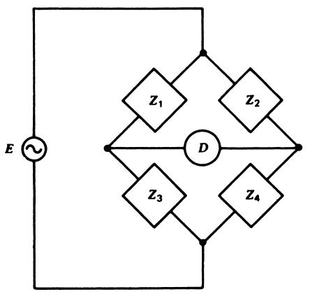
AC Bridges
Same idea as DC bridge, but impedances \(Z_1, Z_2, Z_3, Z_4\) and AC excitation \(E\) .
Offset (phasor) voltage:
\[
\Delta E = E\frac{Z_3Z_2 - Z_1Z_4}{(Z_1 + Z_3)(Z_2 + Z_4)}
\tag{20}
\]
\[
Z_3 Z_2 = Z_1 Z_4
\tag{21}
\]
Special note: if the detector is phase sensitive, both in‑phase and quadrature components must be nulled.
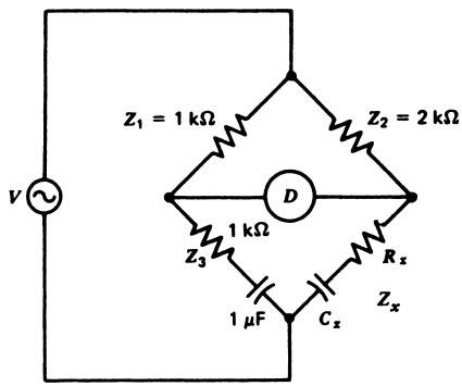
Example 10 — Finding Unknown R and C from an AC Bridge
Assume:
\(Z_1 = R_1\) , \(Z_2 = R_2\) , \(Z_3 = R_3 - j/\omega C\) , \(Z_x = R_x - j/(\omega C_x)\) .
At null: \(Z_2 Z_3 = Z_1 Z_x\) .
Real and imaginary parts must match:
\[
R_x = \frac{R_2 R_3}{R_1}
\]
\[
C_x = C\frac{R_1}{R_2}
\]
With numbers given in the original text:
\(R_x = 2\ \text{k}\Omega\) .\(C_x = 0.5\ \mu\text{F}\) .
Nonlinearity of Bridge Response
Equation (7) is nonlinear in any resistor.
If sensor resistance varies over a wide range , bridge voltage vs resistance is significantly curved (Figure 12a).
If resistance variation is small and centered on the null (e.g., 90–110 Ω around 100 Ω):
The curve is almost linear over that small range (Figure 12b).
We can amplify the small off‑null voltage to expand the scale.
Design tip: operate bridges close to null and limit sensor range to maintain approximate linearity, then do software calibration if needed.
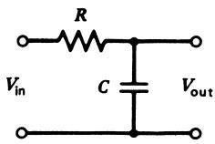
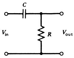
3.3 RC Filters — Basics
Simple first‑order filters built from one R and one C :
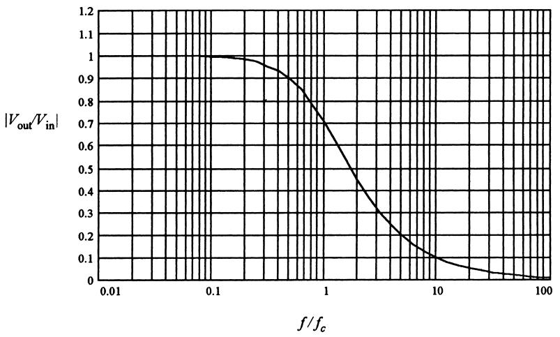
Low-pass (Figure 13): passes DC/low frequencies, attenuates high frequencies.High-pass (Figure 15): passes high frequencies, attenuates low frequencies.
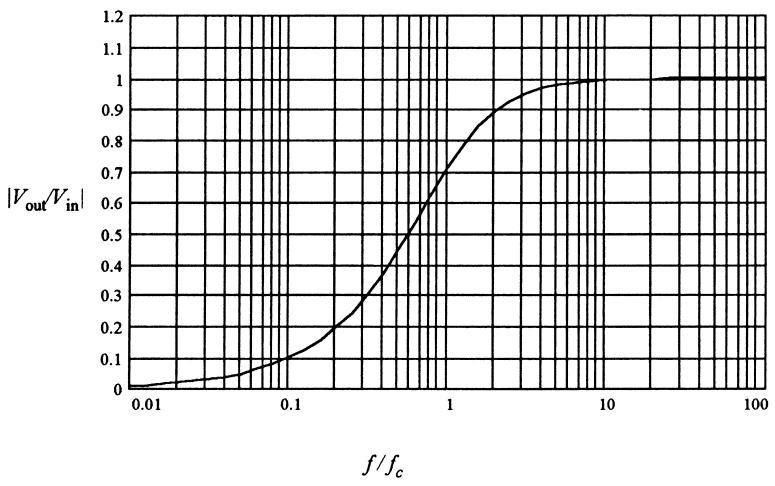
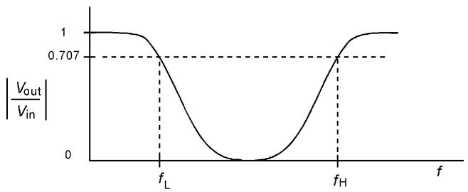
Critical / cutoff frequency:
\[
f_c = \frac{1}{2\pi RC}
\tag{22}
\]
At \(f = f_c\) :
\(|V_{\text{out}}/V_{\text{in}}| = 1/\sqrt{2} \approx 0.707\) → −3 dB point.
Low-Pass RC Filter
Transfer magnitude:
\[
\left| \frac{V_{\text{out}}}{V_{\text{in}}} \right| =
\frac{1}{\sqrt{1 + (f/f_c)^2}}
\tag{23}
\]
Applications:
Measure DC or slowly varying signals while rejecting high‑frequency noise.
Anti‑aliasing before an ADC (though often higher‑order filters are used).
Example 11 — Low-Pass Filter for 1 MHz Noise
Goal:
Measurement signal frequencies < 1 kHz.
Unwanted noise around 1 MHz.
Want noise at 1 MHz attenuated to 1% (\(|V_{\text{out}}/V_{\text{in}}| = 0.01\) ).
What is effect on desired 1 kHz signal?
Use Equation (23):
Set \(f = 1\ \text{MHz}\) , \(|V_{\text{out}}/V_{\text{in}}| = 0.01\) :
\[
0.01 = \frac{1}{\sqrt{1 + (10^6/f_c)^2}}
\Rightarrow (10^6/f_c)^2 \approx 9999
\]
So \(f_c \approx 10\ \text{kHz}\) .
Pick \(C = 0.01\ \mu\text{F}\) ⇒
\[
R = \frac{1}{2\pi f_c C} \approx 1591\ \Omega
\]
Use standard \(R = 1.5\ \text{k}\Omega\) ⇒ actual \(f_c \approx 10.6\ \text{kHz}\) .
Noise attenuation at 1 MHz: very close to 0.01 (slightly better).
Effect on 1 kHz signal:
\[
\left| \frac{V_{\text{out}}}{V_{\text{in}}} \right| =
\frac{1}{\sqrt{1 + (1000/10610)^2}} \approx 0.996
\]
Only about 0.4% loss in the desired band.
Highlight the design trade‑off: place \(f_c\) comfortably above signal band yet far below noise frequency.
High-Pass RC Filter
Transfer magnitude:
\[
\left| \frac{V_{\text{out}}}{V_{\text{in}}} \right| =
\frac{f/f_c}{\sqrt{1 + (f/f_c)^2}}
\tag{24}
\]
At \(f = f_c\) → \(|V_{\text{out}}/V_{\text{in}}| = 0.707\) (−3 dB).
Applications:
Remove DC offsets or low‑frequency drift from signals.
AC‑coupled amplifiers; pulse transmission.
Example 12 — High-Pass Filter for 60 Hz Noise
Goal:
Pulses for a stepper motor at 2000 Hz.
60 Hz noise present.
Want to reduce 60 Hz noise strongly, but allow pulse amplitude to be reduced by no more than 3 dB (≈0.707).
Since 3 dB corresponds to \(|V_{\text{out}}/V_{\text{in}}| = 0.707\) , we choose:
\(f_c = 2000\ \text{Hz}\) .
Now effect on 60 Hz:
\[
\left| \frac{V_{\text{out}}}{V_{\text{in}}} \right|
= \frac{60/2000}{\sqrt{1 + (60/2000)^2}} \approx 0.03
\]
So 60 Hz noise is reduced to about 3% (97% attenuation).
Design: pick \(C = 0.01\ \mu\text{F}\) →
\[
R = \frac{1}{2\pi f_c C} \approx 7.96\ \text{k}\Omega
\]
Choose standard 7.5 kΩ or 8.2 kΩ as close approximations.
Example 13 — 1 vs 2 High-Pass Stages
Goal:
2 kHz data signal contaminated by 60 Hz noise.
Want 60 dB attenuation of 60 Hz (\(|V_{\text{out}}/V_{\text{in}}| = 10^{-3}\) ).
Single-stage high-pass
Use Equation (24):
\[
0.001 = \frac{60/f_c}{\sqrt{1 + (60/f_c)^2}}
\]
Solve → \(f_c \approx 60\ \text{kHz}\) .
Effect on 2 kHz data:
\[
\left|\frac{V_{\text{out}}}{V_{\text{in}}}\right|
= \frac{2000/60000}{\sqrt{1 + (2000/60000)^2}} \approx 0.033
\]
Only 3.3% of data amplitude remains → too much attenuation.
Two cascaded stages (same \(f_c\) )
Overall response ≈ (Equation 24)\(^2\) .
For same 60 dB attenuation of 60 Hz noise, solve:
\[
0.001 = \frac{(60/f_c)^2}{1 + (60/f_c)^2}
\]
→ \(f_c \approx 1896\ \text{Hz}\) .
Now effect on 2 kHz signal (using squared response):
\[
\left|\frac{V_{\text{out}}}{V_{\text{in}}}\right|
= \frac{(2000/1896)^2}{1 + (2000/1896)^2} \approx 0.53
\]
So about 53% of signal remains, much better than 3.3%.
Example 14 — Loading Between Cascaded RC Stages
We now consider loading for Example 13 with specific component choices.
Given:
First stage: choose \(C = 0.001\ \mu\text{F}\) ; need \(f_c = 1896\ \text{Hz}\) .
From \(f_c = 1/(2\pi RC)\) :
\[
R = \frac{1}{2\pi f_c C} \approx 83.9\ \text{k}\Omega
\]
Second stage uses same \(R\) and \(C\) .
Evaluate loading effect at \(f = 2\ \text{kHz}\) .
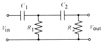
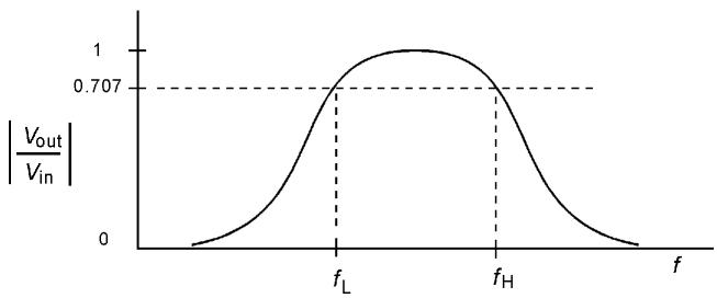
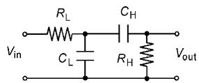
Band-Pass RC Filters
Constructed by cascading a high-pass and a low-pass filter.
Lower critical frequency \(f_L\) from high-pass; upper critical frequency \(f_H\) from low-pass.
Passband is \(f_L < f < f_H\) .
For the RC band‑pass in Figure 20 (including loading via ratio \(r = R_H / R_L\) ):
\[
\left|\frac{V_{\text{out}}}{V_{\text{in}}}\right| =
\frac{f_H f}
{\sqrt{(f^2 - f_H f_L)^2 + [f_L + (1 + r)f_H]^2 f^2}}
\tag{25}
\]
with
\[
f_H = \frac{1}{2\pi R_L C_L}, \quad
f_L = \frac{1}{2\pi R_H C_H}
\tag{26}
\]
Design tips:
Want wide separation between \(f_L\) and \(f_H\) .
Keep \(r = R_H / R_L \le 0.01\) to minimize loading effects.
Example 15 — Band-Pass for 6–60 kHz Data
Goal:
Signal frequencies: 6 kHz to 60 kHz.
Noise at 120 Hz and 1 MHz.
Design RC band‑pass to reduce noise by 90% (|Vout/Vin| = 0.1).
Lower cutoff (high-pass part)
At 120 Hz, want |Vout/Vin| ≈ 0.1:
Use Equation (24):
\[
0.1 = \frac{120/f_L}{\sqrt{1 + (120/f_L)^2}} \Rightarrow f_L \approx 1200\ \text{Hz}
\]
Upper cutoff (low-pass part)
At 1 MHz, want |Vout/Vin| ≈ 0.1:
Use Equation (23):
\[
0.1 = \frac{1}{\sqrt{1 + (10^6/f_H)^2}} \Rightarrow f_H \approx 100\ \text{kHz}
\]
Plot of Equation (25) (Figure 21 in text) shows:
For \(r = 0.1\) vs \(r = 0.01\) , loaded passband is lower in amplitude for larger \(r\) .
Design with \(r = 0.01\) :
Choose \(R_L = 100\ \text{k}\Omega\) , then \(R_H = rR_L = 1\ \text{k}\Omega\) .
From Equation (26):
\(C_H = 0.133\ \mu\text{F}\) .\(C_L = 15.9\ \text{pF}\) .
Effect on data:
At 6 kHz: |Vout/Vin| ≈ 0.969 (3% reduction).
At 60 kHz: |Vout/Vin| ≈ 0.851 (15% reduction).
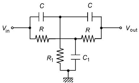
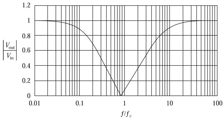
Band-Reject (Notch) Filters
Reject a range of frequencies (especially a narrow band).
Useful when one particular frequency interferes, e.g., 50/60 Hz hum in audio or ECG.
Passive RC implementation with good performance is hard; inductive or active filters usually better.
Twin-T Notch Filter
Configuration:
Top T: series–parallel of R and C.
Bottom T: R and C interchanged.
Grounding components \(R_1\) and \(C_1\) tune the notch.
For \(R_1 = \frac{\pi R}{10}\) and \(C_1 = \frac{10C}{\pi}\) :
\[
f_n = 0.785 f_c, \quad \text{where } f_c = \frac{1}{2\pi RC}
\tag{27}
\]
Frequencies for −3 dB (0.707):
\[
f_L = 0.187 f_c, \quad f_H = 4.57 f_c
\tag{28}
\]
At \(f_n\) , |Vout/Vin| ≈ 0.002 ⇒ good but not perfect rejection.
Example 16 — 400 Hz Notch Filter (Twin-T)
Goal:
On an aircraft, 400 Hz is the power frequency.
Want to reject 400 Hz.
Evaluate effect on voice band (10–300 Hz) and find upper −3 dB frequency.
We want \(f_n = 400\ \text{Hz}\) . From Equation (27):
\[
400 = 0.785 f_c \Rightarrow f_c \approx 510\ \text{Hz}
\]
Pick \(C = 0.01\ \mu\text{F}\) →
\[
R = \frac{1}{2\pi f_c C} \approx 31.2\ \text{k}\Omega
\]
Grounding components:
\[
R_1 = \frac{\pi R}{10} \approx 9800\ \Omega
\]
\[
C_1 = \frac{10C}{\pi} \approx 0.0318\ \mu\text{F}
\]
Effect on voice band:
At 10 Hz: \(10/400 = 0.025\) → from Figure 24, |Vout/Vin| ≈ 0.99 (little attenuation).
At 300 Hz: \(300/400 = 0.75\) → |Vout/Vin| ≈ 0.03 (significant attenuation).
Upper −3 dB frequency:
From Equation (28): \(f_H = 4.57 f_c ≈ 2300\ \text{Hz}\) .
So: - Very good rejection at 400 Hz. - Low voice frequencies largely unaffected, higher low frequencies more attenuated.
Mention that in practice, active notch filters using op‑amps provide deeper notches and more controllable Q factor. Twin‑T is still useful conceptually and in simple analog designs.
Summary / Key Points
Signal conditioning bridges the gap between raw sensor outputs and the requirements of downstream electronics (amplifiers, ADCs, transmitters).Key tasks:
Signal-level & bias changes : match sensor outputs to required voltage ranges.Linearization : historically analog, now often done in software.Conversions : R→V, V↔︎I, analog→digital interface.Filtering : low-pass, high-pass, band-pass, band-reject/notch.Impedance matching & loading mitigation : maintain accuracy.
Loading :
Real sources have internal resistance.
When load is not ≫ source resistance, measured voltage drops (Thévenin model).
Passive circuits :
Voltage dividers: simple R→V conversion but nonlinear, have finite output impedance, dissipate power.
Wheatstone bridges: highly sensitive resistance measurement and R→V conversion; null condition independent of supply.
AC bridges: extend bridges to impedances (R, C, L), account for magnitude and phase.
RC filters :
First‑order low-pass and high-pass with cutoff \(f_c = 1/(2\pi RC)\) .
Easy to design but limited slope (−20 dB/decade).
Cascading increases slope but requires attention to loading.
Band-pass = high-pass + low-pass; band-reject (notch) can be implemented with twin‑T for narrow band rejection.
In modern systems, analog conditioning and digital processing complement each other :
Analog front‑end: scaling, basic filtering, protecting ADC.
Digital side: precise calibration, linearization, advanced filtering.
Wheatstone bridge (DC)
\[
V_a = \frac{V R_3}{R_1 + R_3}, \quad
V_b = \frac{V R_4}{R_2 + R_4}
\]
\[
\Delta V = V_a - V_b =
V\frac{R_3R_2 - R_1R_4}{(R_1 + R_3)(R_2 + R_4)}
\tag{7}
\]
\[
R_3 R_2 = R_1 R_4
\tag{8}
\]
Bridge Thévenin equivalent
\[
V_{\text{Th}} = \Delta V
\tag{9}
\]
\[
R_{\text{Th}}
= \frac{R_1R_3}{R_1 + R_3} + \frac{R_2R_4}{R_2 + R_4}
\tag{10}
\]
\[
I_G = \frac{V_{\text{Th}}}{R_{\text{Th}} + R_G}
\tag{11}
\]
Current-balance bridge
\[
V_b = \frac{V(R_4 + R_5)}{R_2 + R_4 + R_5} + I R_5
\tag{14}
\]
\[
\Delta V = V_a - V_b
= \frac{V R_3}{R_1 + R_3} - \frac{V(R_4 + R_5)}{R_2 + R_4 + R_5} - I R_5
\tag{15}
\]
For potential measurement with properly chosen resistors:
\[
V_x - I R_5 = 0
\tag{19}
\]
AC bridge
\[
\Delta E = E\frac{Z_3Z_2 - Z_1Z_4}{(Z_1 + Z_3)(Z_2 + Z_4)}
\tag{20}
\]
\[
Z_3 Z_2 = Z_1 Z_4
\tag{21}
\]
RC filters
Cutoff frequency (low-pass & high-pass):
\[
f_c = \frac{1}{2\pi RC}
\tag{22}
\]
\[
\left| \frac{V_{\text{out}}}{V_{\text{in}}} \right|
= \frac{1}{\sqrt{1 + (f/f_c)^2}}
\tag{23}
\]
\[
\left| \frac{V_{\text{out}}}{V_{\text{in}}} \right|
= \frac{f/f_c}{\sqrt{1 + (f/f_c)^2}}
\tag{24}
\]
Band-pass RC (including loading, \(r = R_H/R_L\) ):
\[
\left| \frac{V_{\text{out}}}{V_{\text{in}}} \right| =
\frac{f_H f}
{\sqrt{(f^2 - f_H f_L)^2 + [f_L + (1 + r)f_H]^2 f^2}}
\tag{25}
\]
with
\[
f_H = \frac{1}{2\pi R_L C_L}, \quad f_L = \frac{1}{2\pi R_H C_H}
\tag{26}
\]
Twin-T notch filter
\[
f_c = \frac{1}{2\pi RC}
\]
\[
f_n = 0.785 f_c
\tag{27}
\]
\[
f_L = 0.187 f_c, \quad f_H = 4.57 f_c
\tag{28}
\]
Analog Signal Conditioning – Interactive Deck
1. Loading: Sensor + Amplifier as a Divider (Pyodide)
Explore Example 1 numerically. The sensor has internal resistance \(R_x\) and the amplifier has input resistance \(R_L\) . The loaded voltage is
\[
V_{\text{in}} = V_T \left(1 - \frac{R_x}{R_x + R_L}\right)
\]
Try changing \(R_L\) and \(R_x\) and see how the amplifier output changes.
Ask students: - Set R_L = 10_000, then to 100_000, then 1_000. - Which case is “good instrumentation practice,” and why?
2. Loading Error vs. Load Resistance (Reactive Plot)
Use a slider to change \(R_L\) and see how the percentage error caused by loading changes.
= Inputs. range (1 , 200 ], step : 1 , value : 10 , label : "Amplifier input resistance RL [kΩ]" }= Inputs. range (0.1 , 20 ], step : 0.1 , value : 5 , label : "Sensor resistance Rx [kΩ]" }= Inputs. range (0.1 , 5 ], step : 0.1 , value : 1.0 , label : "Sensor open-circuit VT [V]" }= Inputs. range (1 , 20 ], step : 1 , value : 10 , label : "Amplifier gain" }
Guide students: “Move the RL slider to match the curve to your chosen Rx and VT; notice that when RL ≫ Rx, error is small.” Also highlight the log scale on RL.
3. Voltage Divider: Nonlinear Sensor-to-Voltage Mapping (Pyodide)
Revisit the divider from Example 2:
\[
V_D = \frac{R_2}{R_1 + R_2} V_s
\]
Here, \(R_2\) is a sensor that changes with the physical variable.
Ask: Is V_D vs R_2 linear in R_2? If the physical variable is proportional to R_2, what does this do to linearity of measurement vs actual variable?
4. Voltage Divider Transfer Curve (Reactive Plot)
Visualize the full curve \(V_D(R_2)\) and relate it to nonlinearity.
= Inputs. range (1 , 50 ], step : 1 , value : 10 , label : "R1 [kΩ]" }= Inputs. range (1 , 10 ], step : 0.5 , value : 5.0 , label : "Vs [V]" }= Inputs. range (1 , 20 ], step : 1 , value : 4 , label : "Sensor R2_min [kΩ]" }= Inputs. range (2 , 50 ], step : 1 , value : 12 , label : "Sensor R2_max [kΩ]" }
Encourage students to adjust R1 and see how the slope and curvature change. Point out that any straight line they “fit” will only be accurate over a small R2 range.
5. Wheatstone Bridge Offset Voltage (Pyodide)
Let’s compute the DC Wheatstone bridge offset:
\[
\Delta V = V\frac{R_3R_2 - R_1R_4}{(R_1 + R_3)(R_2 + R_4)}
\]
6. Wheatstone Bridge ΔV vs Sensor Resistance (Reactive Plot)
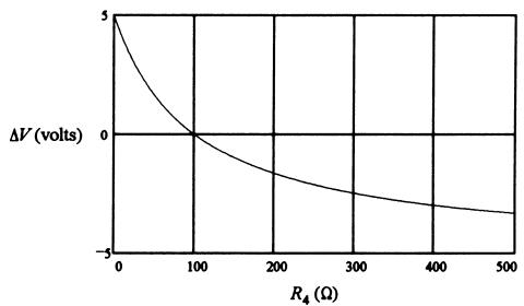
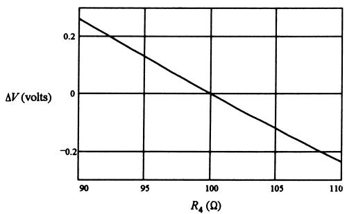
Visualize bridge nonlinearity: how ΔV changes with sensor resistance \(R_4\) .
= Inputs. range (50 , 500 ], step : 10 , value : 100 , label : "R1 [Ω]" }= Inputs. range (50 , 500 ], step : 10 , value : 100 , label : "R2 [Ω]" }= Inputs. range (50 , 500 ], step : 10 , value : 100 , label : "R3 [Ω]" }= Inputs. range (1 , 20 ], step : 1 , value : 10 , label : "Bridge supply V [V]" }= Inputs. range (10 , 500 ], step : 5 , value : 0 , label : "R4_min [Ω] (sensor)" }= Inputs. range (50 , 1000 ], step : 10 , value : 500 , label : "R4_max [Ω] (sensor)" }
Ask students to zoom into a small region around the null (where ΔV ≈ 0) and see that the curve looks almost linear there. This reinforces the “small‑signal linear” region concept.
7. Low-Pass RC Filter Magnitude Response (Pyodide)
Recall:
Cutoff frequency: \(f_c = \dfrac{1}{2\pi RC}\) .
Magnitude response:
\[
\left|\frac{V_{\text{out}}}{V_{\text{in}}}\right| =
\frac{1}{\sqrt{1 + (f/f_c)^2}}
\]
Explore numerically.
Encourage students to modify R and C so that fc moves below or above the test frequencies; observe how |Vout/Vin| changes.
8. Low-Pass RC Bode Magnitude Plot (Reactive Plot)
Interactive plot of \(|V_{\text{out}}/V_{\text{in}}|\) vs \(f\) (log scale), with adjustable R and C.
= Inputs. range (100 , 100_000 ], step : 100 , value : 1_500 , label : "R [Ω] (low-pass)" }= Inputs. range (0.1 , 1000 ], step : 0.1 , value : 10.0 , label : "C [nF] (low-pass)" }
9. High-Pass RC Magnitude Response (Reactive Plot)
For high-pass:
\[
\left|\frac{V_{\text{out}}}{V_{\text{in}}}\right| =
\frac{f/f_c}{\sqrt{1 + (f/f_c)^2}}
\]
= Inputs. range (100 , 100_000 ], step : 100 , value : 8_000 , label : "R [Ω] (high-pass)" }= Inputs. range (0.1 , 1000 ], step : 0.1 , value : 10.0 , label : "C [nF] (high-pass)" }
Relate this to Example 12 and 13: e.g., set fc ≈ 2 kHz and observe attenuation at 60 Hz vs 2 kHz.
10. Band-Pass from Cascaded High-Pass and Low-Pass (Reactive)
Model a simple band-pass as:
\[
H_{\text{BP}}(f) = H_{\text{HP}}(f) \cdot H_{\text{LP}}(f)
\]
with the first-order formulas for each.
= Inputs. range (10 , 100_000 ], step : 10 , value : 1_200 , label : "High-pass cutoff fL [Hz]" }= Inputs. range (1_000 , 500_000 ], step : 1_000 , value : 100_000 , label : "Low-pass cutoff fH [Hz]" }
Connect to Example 15: - Try fL ≈ 1.2 kHz and fH ≈ 100 kHz. - Check attenuation at 120 Hz and 1 MHz; compare to ~0.1 (−20 dB).
11. Twin-T Notch: Frequency Mapping (Pyodide)
For a Twin‑T notch:
\(f_c = \dfrac{1}{2\pi RC}\) .Notch frequency: \(f_n = 0.785 f_c\) .
−3 dB frequencies: \(f_L = 0.187 f_c\) , \(f_H = 4.57 f_c\) .
Compute these for given R and C.
Let students set R and C so that fn ≈ 400 Hz as in Example 16, and check fL and fH.
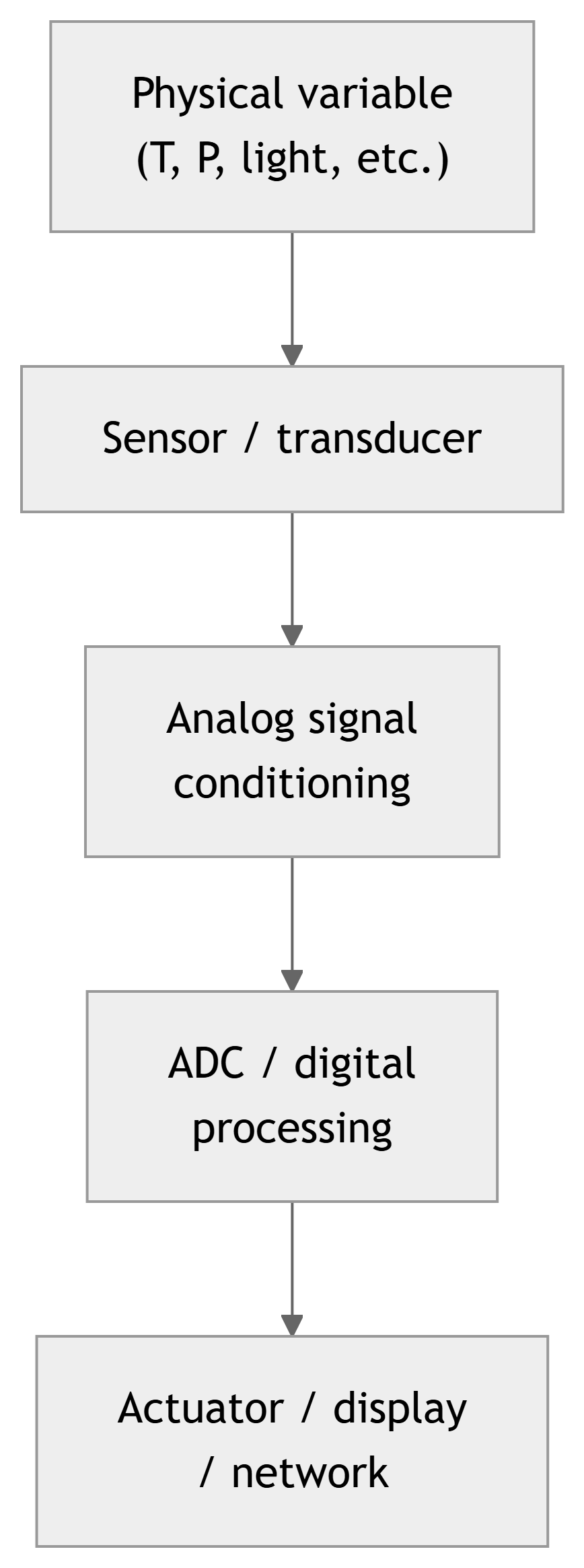
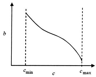
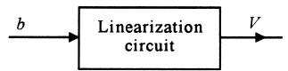
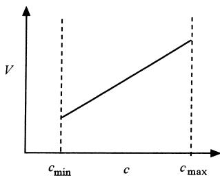
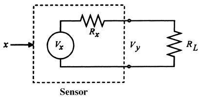
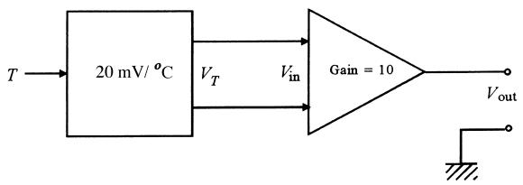
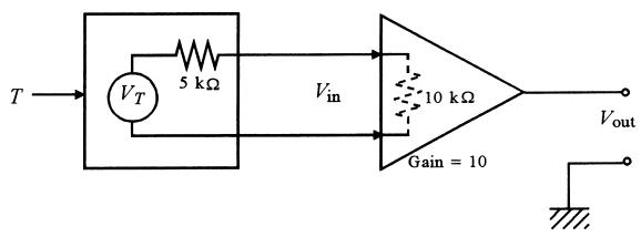 Figure 3: (a) Naive model ignoring loading. (b) Correct model including sensor output resistance and amplifier input resistance.