Electrical Network Transfer Functions
Control 2.2
Learning Objectives
By the end of this section, you will be able to:
Use Laplace-domain impedance and admittance to model R, L, C components.
Derive transfer functions for simple RLC circuits using:
Differential equations
Mesh (loop) analysis
Nodal analysis
Voltage division
Write mesh and node equations for multi-loop / multi-node circuits by inspection.
Derive transfer functions for inverting and noninverting op-amp circuits.
Recognize how these circuit transfer functions become building blocks in control systems (e.g., PID controllers).
Emphasize to students that this section is the “bridge” between basic circuit analysis and control systems.
We are not just solving circuits; we are systematically getting from physical circuits to transfer functions, which later plug directly into block diagrams and control design software.
Big Picture: Why We Care About Transfer Functions in ECE
A transfer function tells us how an input signal \(U(s)\) affects an output signal \(Y(s)\) in the Laplace domain.
For circuits, typical inputs: source voltages or currents.
Typical outputs: voltages across elements, branch currents, etc.
Once we have \(G(s) = \dfrac{Y(s)}{U(s)}\) , we can:
Analyze stability and transient behavior.
Design controllers (like PID) around them.
Simulate entire systems in MATLAB/Simulink.
Think of the transfer function as a “black-box equation” describing your circuit’s behavior.
Later, multiple black boxes will be connected to form full control systems.
Connect this with what students have already seen: step response, eigenvalues, poles/zeros.
Also mention that RLC filters and op-amp circuits they saw in circuits courses are special cases of what they are now formalizing via transfer functions.
Fundamental R, L, C Relationships (Time Domain)
Briefly review these as “known” from basic circuits, but stress we’ll now connect them systematically to Laplace-domain models.
Mention the zero-initial-condition assumption explicitly: this is crucial for using simple \(Z(s)\) expressions.
Table: R, L, C Relationships (Zero Initial Conditions)
Time-domain and impedance/admittance relationships
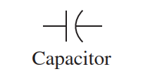
Capacitor
\(v(t) = \dfrac{1}{C}\displaystyle\int_{0}^{t} i(\tau)\,d\tau\) \(i(t) = C \dfrac{dv(t)}{dt}\) \(v(t) = \dfrac{1}{C} q(t)\) \(\dfrac{1}{Cs}\) \(Cs\)
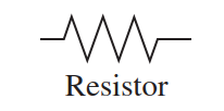
Resistor
\(v(t) = R\,i(t)\) \(i(t) = \dfrac{1}{R} v(t)\) \(v(t) = R \dfrac{dq(t)}{dt}\) \(R\) \(\dfrac{1}{R} = G\)
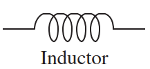
Inductor
\(v(t) = L \dfrac{di(t)}{dt}\) \(i(t) = \dfrac{1}{L}\displaystyle\int_{0}^{t} v(\tau)\,d\tau\) \(v(t) = L \dfrac{d^{2}q(t)}{dt^{2}}\) \(Ls\) \(\dfrac{1}{Ls}\)
Zero initial conditions are assumed for the impedance formulas. If \(i(0^-)\) or \(v(0^-)\) is nonzero, extra terms appear in the Laplace transform.
Point out that the integral limits in the original text had typos (0 to 1); we correct to 0 to \(t\) .
Stress: impedance expressions \(Z_C = 1/(Cs)\) , \(Z_L = Ls\) are the key to building “transformed circuits” in the \(s\) -domain.
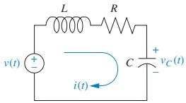
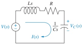
Example 2.6 – Series RLC: Circuit and Goal
Problem
\[
\frac{V_C(s)}{V(s)}
\]
Assume zero initial conditions.
Ask students: “What other choices could we have made for the output?” (inductor voltage, resistor voltage, current).
Relate to control: \(v_C(t)\) could be a sensor voltage representing temperature, position, etc.
Example 2.6 – Step 1: KVL and Integro-Differential Equation
Using KVL around the loop:
\[
L\frac{di(t)}{dt} + R i(t) + \frac{1}{C}\int_{0}^{t} i(\tau)\,d\tau = v(t)
\]
Use current–charge relationship:
\[
i(t) = \frac{dq(t)}{dt}
\]
Substitute into KVL:
\[
L\frac{d^{2}q(t)}{dt^{2}} + R\frac{dq(t)}{dt} + \frac{1}{C}q(t) = v(t)
\]
Highlight the appearance of a 2nd-order ODE: this is why RLC circuits are natural examples for 2nd-order system behavior (oscillation, damping, etc.).
We temporarily use \(q(t)\) just to leverage simpler capacitor relations.
Example 2.6 – Step 2: Express in Terms of Capacitor Voltage
For the capacitor, voltage–charge relationship:
\[
q(t) = C\,v_C(t)
\]
Substitute into the ODE:
\[
LC\frac{d^{2}v_C(t)}{dt^{2}} + RC\frac{dv_C(t)}{dt} + v_C(t) = v(t)
\]
Now both input and output are voltages, which is convenient for transfer functions.
Emphasize the modeling step: translating the loop equation into an ODE relating input \(v(t)\) and output \(v_C(t)\) .
Students should see how choices of state variable (current, charge, voltage) are flexible as long as they are related.
Impedance in the Laplace Domain
Take Laplace transforms of time-domain voltage–current relations (zero initial conditions):
\[
v(t) = \frac{1}{C}\int_{0}^{t} i(\tau)\,d\tau \quad \Rightarrow \quad V(s) = \frac{1}{Cs}I(s)
\]
\[
v(t) = R i(t) \quad \Rightarrow \quad V(s) = R I(s)
\]
\[
v(t) = L \frac{di(t)}{dt} \quad \Rightarrow \quad V(s) = Ls I(s)
\]
Define impedance :
\[
Z(s) \equiv \frac{V(s)}{I(s)}
\]
Thus:
\(Z_C(s) = \dfrac{1}{Cs}\) \(Z_R(s) = R\) \(Z_L(s) = Ls\)
Impedance generalizes resistance to dynamic components (C and L). It captures frequency-dependent behavior in a single algebraic expression.
Relate to phasor analysis: \(Z(j\omega)\) for sinusoidal steady state is analogous, but here \(s\) is a complex variable (not restricted to \(j\omega\) ).
Highlight that once we move to \(Z(s)\) , we can solve circuits exactly like DC resistive networks, just with symbolic impedances.
Transforming the RLC Circuit to the \(s\) -Domain
Starting from the RLC loop equation in the \(s\) -domain:
\[
\left(Ls + R + \frac{1}{Cs}\right) I(s) = V(s)
\]
This has the form:
\[
[\text{Sum of impedances}]\,I(s) = [\text{Sum of applied voltages}]
\]
Example 2.7 – Same RLC, Mesh (Loop) Analysis in \(s\) -Domain
From Figure 2.5:
KVL in \(s\) -domain:
\[
\left(Ls + R + \frac{1}{Cs}\right) I(s) = V(s)
\]
Solve for current:
\[
\frac{I(s)}{V(s)} = \frac{1}{Ls + R + \frac{1}{Cs}}
\]
Capacitor voltage:
\[
V_C(s) = I(s) \cdot Z_C(s) = I(s)\cdot \frac{1}{Cs}
\]
Therefore:
\[
\frac{V_C(s)}{V(s)} = \frac{1}{Cs}\cdot \frac{1}{Ls + R + \frac{1}{Cs}}
\]
Algebraic simplification recovers the same transfer function as in Example 2.6.
By working directly with \(Z(s)\) , we bypass writing and transforming the differential equation. This becomes essential for more complex networks.
Ask: “Which method do you find conceptually clearer?” Some will like the time-domain ODE, others the algebra.
Encourage students to be fluent in both views but to solve exam / design problems using the transformed-circuit shortcut.
Example 2.8 – Single Node via Nodal Analysis
Use Figure 2.5 again, but now apply KCL at the node with voltage \(V_C(s)\) .
Assume:
Currents leaving the node are positive, entering are negative.
Currents:
Through capacitor: \(\displaystyle I_C(s) = \frac{V_C(s)}{1/(Cs)} = Cs\,V_C(s)\)
Through \(R\) –\(L\) series branch (from \(V_C\) to source node at \(V\) ):
\[
I_{RL}(s) = \frac{V_C(s) - V(s)}{R + Ls}
\]
KCL at node \(V_C(s)\) (sum of leaving currents = 0):
\[
\frac{V_C(s)}{1/Cs} + \frac{V_C(s) - V(s)}{R + Ls} = 0
\]
Solve this equation for \(\dfrac{V_C(s)}{V(s)}\) ; the result again matches Example 2.6.
Highlight that in nodal analysis, admittance \(Y = 1/Z\) is often more convenient than impedance.
Remind: this is purely an algebraic equation in \(s\) —no explicit derivatives or integrals now.
Example 2.9 – Voltage Division in the \(s\) -Domain
Same RLC transformed circuit: series combination of \(Z_L(s)\) , \(Z_R(s)\) , and \(Z_C(s)\) .
Voltage division:
\[
V_C(s) = \frac{Z_C(s)}{Z_L(s) + Z_R(s) + Z_C(s)} \, V(s)
= \frac{\dfrac{1}{Cs}}{Ls + R + \dfrac{1}{Cs}}\,V(s)
\]
Thus:
\[
\frac{V_C(s)}{V(s)} = \frac{1/Cs}{Ls + R + 1/Cs}
\]
Algebra gives the same transfer function as before.
Three different methods (ODE, mesh, nodal/voltage division) all give the same \(G(s)\) . Choosing the fastest correct method is a key engineering skill.
Use this as a checkpoint: quickly quiz students—“Which method would you use on an exam and why?”
Transition: simple circuits are fine with any of these; complex circuits demand a systematic mesh/nodal approach.
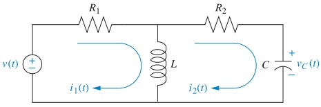
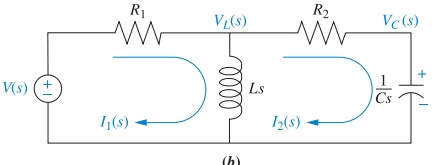
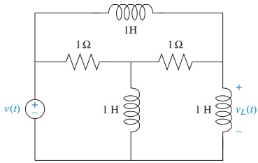
Example 2.10 – Two-Loop Transfer Function via Mesh Analysis
Given
Network of Figure 2.6(a).
Input: \(V(s)\) .
Output: loop 2 current \(I_2(s)\) .
Goal
\[
G(s) = \frac{I_2(s)}{V(s)}
\]
Explain figure (b) carefully: all resistors and inductor now shown as \(R_1\) , \(R_2\) , \(Ls\) , capacitor as \(1/(Cs)\) .
Goal is to show how straightforward it is to write mesh equations in \(s\) -domain, then solve for \(I_2 / V\) .
Example 2.10 – Mesh Equations
Assume mesh currents \(I_1(s)\) and \(I_2(s)\) as shown.
Mesh 1 (around left loop):
\[
R_1 I_1(s) + Ls I_1(s) - Ls I_2(s) = V(s)
\]
Mesh 2 (around right loop):
\[
Ls I_2(s) + R_2 I_2(s) + \frac{1}{Cs} I_2(s) - Ls I_1(s) = 0
\]
Combine terms:
\[
(R_1 + Ls) I_1(s) - Ls I_2(s) = V(s)
\]
\[
- Ls I_1(s) + \left(Ls + R_2 + \frac{1}{Cs}\right) I_2(s) = 0
\]
Ask students to identify:
“Self-impedance” terms on the diagonal (sum of all impedances around each mesh).
“Mutual impedance” terms (common elements with opposite sign).
This pattern leads to the inspection technique later.
Example 2.10 – Solving by Cramer’s Rule
Write the system in matrix form:
\[
\begin{bmatrix}
R_1 + Ls & -Ls \\
-Ls & Ls + R_2 + \dfrac{1}{Cs}
\end{bmatrix}
\begin{bmatrix}
I_1(s) \\ I_2(s)
\end{bmatrix}
=
\begin{bmatrix}
V(s) \\ 0
\end{bmatrix}
\]
Let the determinant:
\[
\Delta =
\begin{vmatrix}
R_1 + Ls & -Ls \\
-Ls & Ls + R_2 + \dfrac{1}{Cs}
\end{vmatrix}
\]
For \(I_2(s)\) , Cramer’s Rule:
\[
I_2(s) = \frac{
\begin{vmatrix}
R_1 + Ls & V(s) \\
-Ls & 0
\end{vmatrix}
}{\Delta}
= \frac{Ls\,V(s)}{\Delta}
\]
So:
\[
G(s) = \frac{I_2(s)}{V(s)} = \frac{Ls}{\Delta}
\]
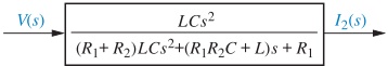
Carrying out determinant algebra yields:
\[
G(s) = \frac{LC s^{2}}{(R_1 + R_2)LC s^{2} + (R_1 R_2 C + L)s + R_1}
\]
(as in Figure 2.6(c)).
You do not need students to memorize the exact polynomial; more important is that they understand how to get it.
Mention that Symbolic Math Toolbox in MATLAB can compute \(G(s)\) automatically from the matrix form.
Mesh-Equation Pattern (Two Loops)
The general form of the two-mesh equations observed:
\[
\left[\text{Sum of impedances around Mesh 1}\right] I_1(s)
- \left[\text{Sum of common impedances}\right] I_2(s)
= \left[\text{Sum of applied voltages around Mesh 1}\right]
\]
\[
- \left[\text{Sum of common impedances}\right] I_1(s)
+ \left[\text{Sum of impedances around Mesh 2}\right] I_2(s)
= \left[\text{Sum of applied voltages around Mesh 2}\right]
\]
Recognizing this structure lets you write mesh equations by inspection without rederiving each term.
Inspection rule for mesh \(k\) :
Diagonal term: sum of all impedances in that mesh.
Off-diagonal term: negative sum of impedances shared with the other mesh.
Prepare students for mechanical systems: inertia, springs, dampers produce the same matrix structure as RLC circuits once written in \(s\) -domain.
This “pattern recognition” is a huge time saver in modeling.
Nodal Analysis and Admittance
Define admittance :
\[
Y(s) = \frac{1}{Z(s)} = \frac{I(s)}{V(s)}
\]
For basic elements:
Capacitor: \(Y_C(s) = Cs\)
Resistor: \(Y_R(s) = 1/R = G\)
Inductor: \(Y_L(s) = 1/(Ls)\)
Using admittance can make KCL equations more compact, especially when multiple parallel branches are present.
Connect to DC nodal analysis: there you used conductances; here it’s the same but now frequency-dependent via \(s\) .
Set up for Example 2.11 where the two-loop network is re-analyzed via nodes.
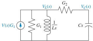
Example 2.11 – Transfer Function via Nodal Analysis
Use the transformed circuit of Figure 2.6(b).
Nodes:
Node at inductor: \(V_L(s)\)
Node at capacitor: \(V_C(s)\)
KCL at \(V_L(s)\) : sum of currents leaving node = 0:
\[
\frac{V_L(s) - V(s)}{R_1} + \frac{V_L(s)}{Ls} + \frac{V_L(s) - V_C(s)}{R_2} = 0
\]
KCL at \(V_C(s)\) :
\[
Cs\,V_C(s) + \frac{V_C(s) - V_L(s)}{R_2} = 0
\]
Express resistances as conductances \(G_1 = 1/R_1\) , \(G_2 = 1/R_2\) :
\[
\left(G_1 + G_2 + \frac{1}{Ls}\right) V_L(s) - G_2 V_C(s) = G_1 V(s)
\]
\[
- G_2 V_L(s) + (G_2 + Cs) V_C(s) = 0
\]
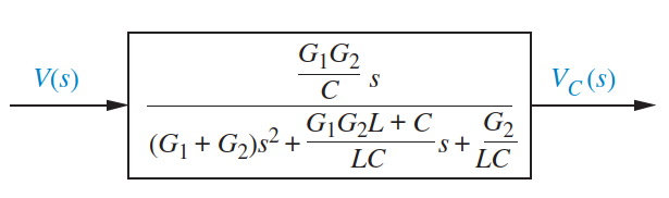
Solve simultaneously for \(V_C(s)/V(s)\) :
\[
\frac{V_C(s)}{V(s)} =
\frac{\dfrac{G_1 G_2}{C} s}{
(G_1 + G_2) s^{2} + \dfrac{G_1 G_2 L + C}{LC} s + \dfrac{G_2}{LC}
}
\]
(as shown in Figure 2.7).
Encourage students to compare this expression with the mesh-based one from Example 2.10.
Both represent the same physical network but with different input–output choices.
Point out how readily admittances appear in the coefficients when using nodal analysis.
Norton Equivalent and Current-Source View
Sometimes nodal analysis is simpler if we convert voltage sources in series with impedances into current sources in parallel with admittances (Norton’s theorem).
Voltage source \(V(s)\) in series with \(Z_s(s)\) \(\Rightarrow\) equivalent current source \(\dfrac{V(s)}{Z_s(s)}\) in parallel with \(Z_s(s)\) (or \(Y_s = 1/Z_s\) ).
This leads to nodal equations of the general form:
\[
\left[\text{Sum of admittances connected to Node 1}\right] V_1(s)
- \left[\text{Common admittances}\right] V_2(s)
= \left[\text{Sum of applied currents at Node 1}\right]
\]
…and similarly for Node 2.
Use this to motivate Example 2.12 where the same two-node network is redrawn in a Norton form.
Stress that this is a modeling choice; physically both circuits are equivalent.
Example 2.12 – Nodal Analysis with Current Sources
Convert all impedances to admittances (\(G_1\) , \(G_2\) , \(Cs\) , \(1/(Ls)\) ).
Convert series voltage sources to equivalent current sources.
KCL at \(V_L(s)\) :
\[
G_1 V_L(s) + \frac{1}{Ls} V_L(s) + G_2\bigl[V_L(s) - V_C(s)\bigr] = G_1 V(s)
\]
KCL at \(V_C(s)\) :
\[
Cs\,V_C(s) + G_2\bigl[V_C(s) - V_L(s)\bigr] = 0
\]
These are algebraically identical to the equations in Example 2.11, thus yielding the same \(V_C(s)/V(s)\) .
Pattern for node equations:
Diagonal term (for node \(k\) ): sum of admittances connected to node \(k\) .
Off-diagonal: negative sum of admittances common to nodes \(k\) and \(\ell\) .
Reinforce the analogy to the mesh pattern: diagonals = self, off-diagonals = negative mutual.
Emphasize: once students see this pattern, they can write equations for large nodal networks very quickly.
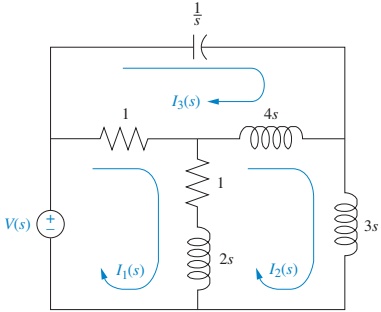
Example 2.13 – Mesh Equations by Inspection (Three Loops)
Goal: Write , but do not solve, the mesh equations.
General structure for Mesh 1:
\[
\bigl[\text{Sum of impedances around Mesh 1}\bigr] I_1(s)
- \bigl[\text{Common impedances (1–2)}\bigr] I_2(s)
- \bigl[\text{Common impedances (1–3)}\bigr] I_3(s)
= \bigl[\text{Sum of applied voltages around Mesh 1}\bigr]
\]
Similarly for Meshes 2 and 3.
After substituting values from Figure 2.9, we obtain:
Mesh 1:
\[
(2s + 2) I_1(s) - (2s + 1) I_2(s) - I_3(s) = V(s)
\]
Mesh 2:
\[
-(2s + 1) I_1(s) + (9s + 1) I_2(s) - 4s\,I_3(s) = 0
\]
Mesh 3:
\[
- I_1(s) - 4s\,I_2(s) + \left(4s + 1 + \frac{1}{s}\right) I_3(s) = 0
\]
These can be solved for any desired transfer function, e.g., \(I_3(s)/V(s)\) .
Recommend that students practice identifying self and mutual impedances by visually circling each mesh and shared branches.
Mention the MATLAB snippet in the text (TryIt 2.8) which uses symbolic matrices to solve these equations.
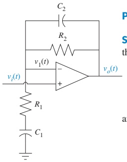
Inverting Op-Amp Configuration
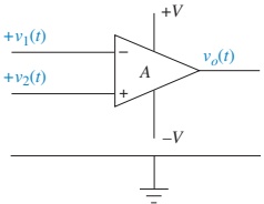
If the non-inverting input is grounded (\(v_2 = 0\) ), we get an inverting amplifier :
\[
v_o(t) = -A v_1(t)
\]
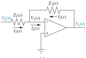
With impedances \(Z_1(s)\) and \(Z_2(s)\) connected as in Figure 2.10(c):
Key consequences of ideal assumptions:
Input current \(I_a(s) = 0\) (no current into op-amp input).
Therefore, \(I_1(s) = -I_2(s)\) through \(Z_1\) and \(Z_2\) .
Large \(A\) forces \(v_1(t) \approx 0\) (virtual ground).
So:
\[
I_1(s) = \frac{V_i(s)}{Z_1(s)}, \quad I_2(s) = \frac{V_o(s)}{Z_2(s)}
\]
From \(I_1 = -I_2\) :
\[
\frac{V_o(s)}{Z_2(s)} = -\frac{V_i(s)}{Z_1(s)}
\Rightarrow
\frac{V_o(s)}{V_i(s)} = -\frac{Z_2(s)}{Z_1(s)}
\]
Inverting op-amp transfer function:
\[
G(s) = \frac{V_o(s)}{V_i(s)} = -\frac{Z_2(s)}{Z_1(s)}
\]
Emphasize the generality: by choosing \(Z_1(s)\) and \(Z_2(s)\) as resistor, capacitor, or their combinations, we can realize many transfer functions.
Preview: Example 2.14 will show how this becomes a PID controller.
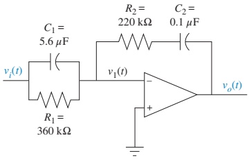
Example 2.14 – Inverting Op-Amp as a PID Controller
We know:
\[
\frac{V_o(s)}{V_i(s)} = -\frac{Z_2(s)}{Z_1(s)}
\]
Compute \(Z_1(s)\) : parallel \(R_1\) and \(C_1\) :
Admittances in parallel add: \(Y_1(s) = C_1 s + \dfrac{1}{R_1}\) .
Therefore:
\[
Z_1(s) = \frac{1}{C_1 s + \dfrac{1}{R_1}}
= \frac{1}{C_1 s + G_1}
\]
(Numerical combination gives: \(Z_1(s) = \dfrac{360\times 10^{3}}{2.016 s + 1}\) in the text.)
Compute \(Z_2(s)\) : series \(R_2\) and \(C_2\) :
\[
Z_2(s) = R_2 + \frac{1}{C_2 s}
\]
Plug into \(-Z_2/Z_1\) and simplify:
\[
\frac{V_o(s)}{V_i(s)} = -1.232 \frac{s^{2} + 45.95 s + 22.55}{s}
\]
This is of the form:
\[
K\left( s + \frac{\text{something}}{s} + 1 \right)
\]
which corresponds to a PID (Proportional–Integral–Derivative) controller .
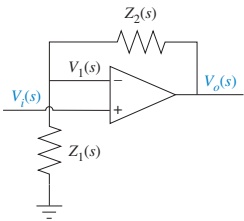
Noninverting Op-Amp Configuration
Input \(V_i(s)\) is applied to the non-inverting terminal.
Feedback network: \(Z_1(s)\) –\(Z_2(s)\) forming a voltage divider.
Op-amp equation:
\[
V_o(s) = A\bigl(V_i(s) - V_1(s)\bigr)
\]
Noninverting Op-Amp Configuration
By voltage division:
\[
V_1(s) = \frac{Z_1(s)}{Z_1(s) + Z_2(s)} V_o(s)
\]
Substitute into op-amp equation:
\[
V_o(s) = A\left[V_i(s) - \frac{Z_1}{Z_1 + Z_2} V_o(s)\right]
\]
Rearrange and solve for \(V_o/V_i\) :
\[
\frac{V_o(s)}{V_i(s)} = \frac{A}{1 + A Z_1(s)/(Z_1(s) + Z_2(s))}
\]
For large \(A\) , the “1” in the denominator is negligible:
\[
\frac{V_o(s)}{V_i(s)} \approx \frac{Z_1(s) + Z_2(s)}{Z_1(s)}
\]
Noninverting op-amp transfer function (large \(A\) ):
\[
G(s) = \frac{V_o(s)}{V_i(s)} = \frac{Z_1(s) + Z_2(s)}{Z_1(s)}
\]
Highlight difference vs inverting case: output is noninverting and gain expression differs.
Again, if \(Z_1\) and \(Z_2\) are frequency-dependent, we get frequency-selective amplifiers and control elements.
Example 2.15 – Noninverting Op-Amp with R–C Networks
Given:
\(Z_1(s) = R_1 + \dfrac{1}{C_1 s}\) (series \(R_1\) and \(C_1\) ).\(Z_2(s) = \dfrac{R_2 \bigl(1/(C_2 s)\bigr)}{R_2 + 1/(C_2 s)}\) (parallel \(R_2\) and \(C_2\) ).
Use:
\[
\frac{V_o(s)}{V_i(s)} = \frac{Z_1(s) + Z_2(s)}{Z_1(s)}
\]
After substituting and simplifying:
\[
\frac{V_o(s)}{V_i(s)} =
\frac{C_2 C_1 R_2 R_1 s^{2} + (C_2 R_2 + C_1 R_2 + C_1 R_1)s + 1}
{C_2 C_1 R_2 R_1 s^{2} + (C_2 R_2 + C_1 R_1)s + 1}
\]
Note that numerator and denominator are very similar; this suggests particular frequency-response characteristics (e.g., some zeros cancel near certain poles).
Students don’t need to memorize this expression; the key is the method: find \(Z_1\) , \(Z_2\) , use the general noninverting formula.
Real-World ECE Application: RLC Filters and Sensors
A series RLC circuit like Example 2.6 can be used as a band-pass filter in audio or communication systems.
The transfer function \(V_C(s)/V(s)\) shapes how different frequencies are passed or attenuated.
In control systems, the same RLC can be part of a sensor conditioning circuit, where \(v_C(t)\) represents a measured physical quantity (e.g., strain gauge + filter).
Designing the resistor, inductor, and capacitor values sets the “dynamic response” (rise time, overshoot) of the measured signal feeding the controller.
Use this slide to connect the math back to hardware: filter design, sensor interfaces, analog front-ends.
Ask: “If we want a faster sensor, which parameter might we reduce — \(L\) , \(C\) , or \(R\) ? What does that do to \(\omega_n\) and damping?”
Summary / Key Points
R, L, C elements have simple Laplace-domain impedances: \(Z_R = R\) , \(Z_L = Ls\) , \(Z_C = 1/(Cs)\) .
We can model circuits in the \(s\) -domain by replacing each element with \(Z(s)\) and applying KVL/KCL just like in DC circuits.
For simple circuits, transfer functions can be obtained via:
Differential equation → Laplace transform.
Mesh analysis (KVL in \(s\) -domain).
Nodal analysis (KCL in \(s\) -domain).
Voltage division using impedances.
For multi-loop / multi-node circuits:
Mesh equations: diagonal terms = sum of mesh impedances; off-diagonals = negative common impedances.
Node equations: diagonal terms = sum of admittances at node; off-diagonals = negative common admittances.
Op-amp circuits (inverting and noninverting) realize transfer functions:
Inverting: \(G(s) = -Z_2(s)/Z_1(s)\) .
Noninverting (large \(A\) ): \(G(s) = [Z_1(s)+Z_2(s)]/Z_1(s)\) .
These circuit transfer functions become building blocks for controllers (e.g., PID) and analog filters in control systems.
Reinforce the unifying theme: once we have \(G(s)\) , we can treat circuits like any other dynamic system (mechanical, thermal, etc.), using the same control tools.
Preview: next, we’ll apply identical modeling ideas to mechanical systems via analogies (force–voltage, velocity–current).
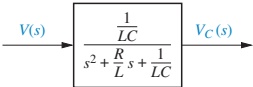
Generic Transfer Function Definition
For input \(U(s)\) and output \(Y(s)\) :
\[
G(s) = \frac{Y(s)}{U(s)}
\]
Series RLC (capacitor output) – Example 2.6
\[
\frac{V_C(s)}{V(s)} = \frac{1/LC}{s^{2} + \dfrac{R}{L}s + \dfrac{1}{LC}}
\]
Series Impedances in Loop Equation
General KVL in \(s\) -domain:
\[
\bigl[\text{Sum of impedances}\bigr] I(s) = \bigl[\text{Sum of sources}\bigr]
\]
Two-Mesh Pattern
\[
\begin{bmatrix}
\sum Z_{\text{Mesh 1}} & -\sum Z_{\text{common}} \\
-\sum Z_{\text{common}} & \sum Z_{\text{Mesh 2}}
\end{bmatrix}
\begin{bmatrix}
I_1(s) \\ I_2(s)
\end{bmatrix}
=
\begin{bmatrix}
\sum V_{\text{Mesh 1}} \\ \sum V_{\text{Mesh 2}}
\end{bmatrix}
\]
Two-Node Pattern (Admittances)
\[
\begin{bmatrix}
\sum Y_{\text{Node 1}} & -\sum Y_{\text{common}} \\
-\sum Y_{\text{common}} & \sum Y_{\text{Node 2}}
\end{bmatrix}
\begin{bmatrix}
V_1(s) \\ V_2(s)
\end{bmatrix}
=
\begin{bmatrix}
\sum I_{\text{Node 1}} \\ \sum I_{\text{Node 2}}
\end{bmatrix}
\]
Op-Amp Transfer Functions
\[
\frac{V_o(s)}{V_i(s)} = -\frac{Z_2(s)}{Z_1(s)}
\]
Noninverting configuration (large \(A\) ):
\[
\frac{V_o(s)}{V_i(s)} = \frac{Z_1(s) + Z_2(s)}{Z_1(s)}
\]
Encourage students to keep this formula slide handy as a reference while doing homework and labs, especially the \(Z(s)\) of R, L, C and the op-amp formulas.
This reduces algebra mistakes and lets them focus on modeling choices and interpretation of \(G(s)\) .
Interactive Agenda
Explore R, L, C impedances in Python (Pyodide).
Experiment with pole locations of an RLC circuit and see their effect on \(G(s)\) .
Compare mesh vs. nodal analysis numerically.
Interactively explore inverting and noninverting op-amp transfer functions.
This addendum is meant to be used after students have seen the main slides.
Encourage them to modify parameters, re-run cells, and observe how circuit behavior changes numerically and graphically.
Interactive: R, L, C Impedance Calculator
Use this live Python block to calculate impedances for R, L, C at a chosen value of \(s = \sigma + j\omega\) .
Reactive: Visualizing R, L, C Magnitudes vs Frequency
Use the sliders to change \(R\) , \(L\) , and \(C\) values, and see how the impedance magnitudes vary with frequency.
= Inputs. range ([10 , 5000 ], {step : 10 , value : 1000 , label : "R (Ω)" })= Inputs. range ([1e-4 , 0.1 ], {step : 1e-4 , value : 1e-2 , label : "L (H)" })= Inputs. range ([1e-9 , 1e-4 ], {step : 1e-9 , value : 1e-6 , label : "C (F)" })
Interactive: Series RLC Transfer Function Coefficients
Recall for the series RLC with capacitor voltage output (Example 2.6):
\[
\frac{V_C(s)}{V(s)} = \frac{1/LC}{s^{2} + \dfrac{R}{L}s + \dfrac{1}{LC}}
\]
Use Python to compute the denominator coefficients for your chosen \(R\) , \(L\) , \(C\) .
Connect: - \(a_0 = \omega_n^2 = 1/(LC)\) . - \(a_1 = 2 \zeta \omega_n = R/L\) .
Students can change \(R\) and see how damping ratio changes qualitatively (although we don’t compute \(\zeta\) explicitly here).
Reactive: Poles of the Series RLC Transfer Function
Interactively vary \(R\) , \(L\) , and \(C\) , and observe the pole locations of:
\[
G(s) = \frac{V_C(s)}{V(s)} = \frac{1/LC}{s^{2} + \frac{R}{L}s + \frac{1}{LC}}
\]
= Inputs. range ([0 , 100 ], {step : 1 , value : 10 , label : "R (Ω)" })= Inputs. range ([1e-4 , 1e-1 ], {step : 1e-4 , value : 1e-3 , label : "L (H)" })= Inputs. range ([1e-9 , 1e-4 ], {step : 1e-9 , value : 1e-6 , label : "C (F)" })
Interactive: Mesh vs. Nodal Equation Coefficients (Conceptual)
For the two-loop mesh system in Example 2.10, the equations:
\[
(R_1 + Ls) I_1(s) - Ls I_2(s) = V(s)
\]
\[
- Ls I_1(s) + \left(Ls + R_2 + \frac{1}{Cs}\right) I_2(s) = 0
\]
Use Python to build the coefficient matrix symbolically for selected \(R_1\) , \(R_2\) , \(L\) , \(C\) at a particular \(s\) .
This reinforces the “pattern” of mesh equations and gives students a symbolic-algebra view.
They can change \(R_1, R_2, L, C\) and see how each term changes the matrix entries.
Reactive: Inverting Op-Amp – Frequency Response Magnitude
For an inverting op-amp:
\[
G(s) = -\frac{Z_2(s)}{Z_1(s)}
\]
Here, choose:
\(Z_1\) as a capacitor \(C_1\) (pure integrator).\(Z_2\) as a resistor \(R_2\) .
Then:
\[
G(s) = -R_2 C_1 s
\]
Magnitude grows linearly with \(\omega\) . Explore this behavior interactively.
= Inputs. range ([1e3 , 1e6 ], {step : 1e3 , value : 1e5 , label : "R2 (Ω)" })= Inputs. range ([1e-8 , 1e-4 ], {step : 1e-8 , value : 1e-5 , label : "C1 (F)" })
Interactive: Noninverting Op-Amp – DC Gain with Resistive Network
For large-\(A\) noninverting op-amp:
\[
G(s) = \frac{Z_1 + Z_2}{Z_1}
\]
Let \(Z_1 = R_1\) and \(Z_2 = R_2\) (purely resistive):
\[
G = 1 + \frac{R_2}{R_1}
\]
Use Python to compute the DC gain for selected resistor values.
Encourage students to try different resistor ratios and connect to amplifier design:
For \(G = 2\) , what ratio \(R_2/R_1\) do we need?
For \(G = 10\) ?
This also links to the special case used often in sensor amplifiers.
Reactive: Noninverting Op-Amp with Simple RC Feedback
Make \(Z_1 = R_1 + 1/(C_1 s)\) and \(Z_2 = R_2\) (for simplicity). Then approximately:
\[
G(s) = \frac{Z_1 + Z_2}{Z_1} = 1 + \frac{R_2}{R_1 + 1/(C_1 s)}
\]
Interactively explore \(|G(j\omega)|\) as \(R_1\) , \(R_2\) , and \(C_1\) vary.
= Inputs. range ([1e3 , 1e6 ], {step : 1e3 , value : 1e4 , label : "R1 (Ω)" })= Inputs. range ([1e3 , 1e6 ], {step : 1e3 , value : 9e4 , label : "R2 (Ω)" })= Inputs. range ([1e-9 , 1e-4 ], {step : 1e-9 , value : 1e-6 , label : "C1 (F)" })
Students can see how adding a capacitor in series with \(R_1\) introduces frequency dependence into the gain.
This is a simple step towards understanding frequency-compensated amplifiers and lead/lag compensators in control.
Wrap-Up Interactive Check
Use the block below as a quick self-check: given \(R\) , \(L\) , \(C\) and the form
\[
G(s) = \frac{1/LC}{s^{2} + \frac{R}{L}s + \frac{1}{LC}},
\]
numerically evaluate \(|G(j\omega)|\) at a chosen frequency.
Encourage students to compare this numeric magnitude with what they see on the pole plot and Bode-like plots earlier.
This ties everything—component values, transfer function form, poles, and numerical frequency response—into a coherent picture.